0 Preface
With the rapid development of high-speed integrated circuits and the wide application of wireless communication systems, electronic equipment is developing towards miniaturization and integration. The emergence of flexible electronics such as flexible electronic skins, flexible pressure sensors, and flexible electrodes has also demonstrated people's demand for flexible and bendable electronic devices. Flexible electronics contain unlimited potential and opportunities.
Polydimethylsiloxane (PDMS) is an organic polymer material with the advantages of cheap raw materials, good chemical stability, good durability, and good biocompatibility [1-4]. It is widely used in many fields such as electronics, micromachines, medicine, biology and so on. Flexible devices based on PDMS have also been reported in domestic and foreign literatures. GUO H[5] et al. designed a flexible orthogonal grating structure on PDMS substrate that can measure vector stress/strain. CUI JL[6] et al. fabricated a flexible capacitor with high sensitivity based on PDMS substrate. RAHMAN HA [7] et al designed a flexible antenna suitable for wearable devices with PDMS as substrate, BISWAS S [8] et al designed a PDMS-based flexible antenna suitable for retinal detection. Multi-array electrodes, Cao Jianguo [9] and others made a highly flexible and elastic electronic skin tactile sensor based on PDMS. All of the above need to design and fabricate a metal structure on the PDMS substrate. Generally, a metal pattern is fabricated on the PDMS substrate. A metal mask with a specific hollow pattern is used as the pattern mask, and the metal layer is deposited by electron beam evaporation or sputtering. Therefore, the precision of the metal pattern directly depends on the precision of the metal mask, but due to the limitation of traditional machining methods, the precision of the metal mask is low and the cost is high. When the electron beam evaporates or sputters the metal layer, the metal mask cannot be guaranteed The close attachment of the reticle to the PDMS substrate can also easily cause problems such as distortion of metal patterns, which cannot meet the stringent requirements for dimensional processing errors of high-resolution graphics or structures that require high precision.
In this paper, based on the current promotion trend of the fifth-generation mobile communication network (5G), the flexible and bendable material PDMS is combined with 5G communication technology. From the exploration of the PDMS-based flexible substrate, the comparison of the use of different photoresist stripping to fabricate micro-fine structures From the perspective of 5G communication system, a small (35 000 μm × 35 000 μm) ultra-wide band (3.3 GHz to 5.0 GHz) MEMS monopole flexible antenna is designed. The antenna uses PDMS material as a flexible dielectric substrate, and a disk-shaped metal radiation structure is designed on one side of the dielectric substrate. Coplanar Waveguide (CPW) is used for feeding, which makes the structure of the antenna more compact. The impedance matching bandwidth of the CPW feed antenna is very sensitive to the dimensional processing error of the metal gap of the CPW structure and the signal conducting strip. A small change in its size will cause a large change in the impedance matching bandwidth. Therefore, a metal mask is used for deposition. The way of the mask is difficult to meet its high precision requirements. In order to reduce the influence of the dimensional processing error of the CPW structure on the performance of the antenna and meet its high-precision requirements, a metal-nickel waveguide feed with a thickness of 500 nm was fabricated on the PDMS flexible substrate with a photoresist as a mask and a metal lift-off process. MEMS flexible antenna. In the experiment, the antenna fed with CPW structure was peeled off with different photoresists as masks, and the effects of CPW peeled off based on different photoresists on the performance of the antenna were analyzed and compared, and the antennas were tested in the free state and the bent state. Test comparison.
1 Structural design of the antenna
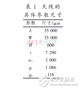
The structure of the small ultra-wideband CPW structure-fed MEMS monopole flexible antenna designed in this paper is shown in Figure 1. It has the characteristics of simple structure, light weight, easy integration, and flexible bending. The antenna uses the flexible material PDMS as the dielectric substrate, its size L×W×H is 35 000 μm×35 000 μm×600 μm, and the relative permittivity ε is 2.68.
The antenna is designed on one side of the PDMS flexible dielectric substrate, and a disk-shaped radiating metal structure with a radius r is designed. The antenna uses a CPW structure with a standard impedance of 50 Ω for feeding. The CPW not only has the advantages of small parasitic parameters, good dispersion characteristics, small radiation loss, and easy integration [10-11], but also can be combined with the disc-shaped antenna of the antenna. The radiating metal structure is integrated on the same side of the substrate, which makes the structure of the antenna more compact and easier to integrate and interconnect with electronic equipment. The CPW structure is located at the symmetrical center of the substrate, and its signal conduction band is connected to the disc-shaped radiating metal structure. The width of the signal conduction band is w1, and the gap between the signal conduction band and the metal ground on both sides of the CPW is g2. The specific parameters of the antenna are shown in Table 1.
2 Preparation of the antenna
2.1 Surface treatment of PDMS
This paper explores the fabrication of CPW-fed MEMS monopole flexible antenna based on PDMS substrate using different photoresist and metal lift-off process. Photoresist needs to be uniformly coated on PDMS, but the untreated PDMS surface has high hydrophobicity and self-cleaning. Due to the characteristics of nature, PDMS substrate cannot be uniformly coated with photoresist under normal conditions, which also limits its wide application. Reference [12] proposed a method to permanently change the hydrophobicity of the PDMS surface. The contact angle between the water droplet and the PDMS surface proved that the PDMS surface was functionalized as hydrophilic. However, photoresist is a complex organic mixture, and water is a pure inorganic compound. Whether the modification method is still suitable for improving the adhesion between photoresist and PDMS surface requires verification experiments.
The three PDMS substrates were treated with oxygen plasma, surfactant (sodium dodecyl sulfate, SDS solution), and combined treatment with SDS immediately after oxygen plasma treatment. Adhesion effect of resist to PDMS surface. Use a micropipette to drop about 20 μL of photoresist on the four samples respectively. The adhesion between PDMS and photoresist is shown in Figure 2. In Figure 2(a), the photoresist droplets converged but did not disperse on the untreated PDMS surface, proving that the PDMS surface was still highly hydrophobic to the organic mixture photoresist; in Figure 2(b), the PDMS surface was treated with the surfactant SDS. However, the photoresist droplets were still in the shape of water droplets on the surface of PDMS, which proved that the modification effect was not good; in Figure 2(c), PDMS was etched by oxygen plasma (power 220 W, oxygen flow 150 SCCM, time 120 s), The photoresist droplets spread along the PDMS surface and adhered to each other, indicating that the PDMS surface was effectively modified to a hydrophilic surface, but within about 30 min, the PDMS surface would return to its original hydrophobic state and could not remain hydrophilic permanently ; In Figure 2(d), after PDMS was etched by oxygen plasma, it was treated with SDS immediately, and it was observed that the photoresist droplets could evenly infiltrate the PDMS surface, realizing the permanent hydrophilic modification of the PDMS surface, which proves this The method can be adapted to improve the adhesion of photoresist to PDMS. To sum up, the PDMS substrates in the following are all treated by oxygen plasma etching and combined treatment with SDS.
2.2 Fabrication of the antenna
In the experiment, a 4-inch silicon wafer was used as the carrier, PDMS was used as the substrate, different photoresists were spin-coated on it, and the mask pattern was developed by photolithography, and then 500 nm metal nickel was sputtered. Metal graphics. In this way, a CPW-fed MEMS flexible monopole antenna was fabricated. In the metal stripping process, the positive adhesive stripping process based on AZ6130 photoresist, the positive adhesive stripping process based on RZJ304 photoresist, and the pattern inversion process based on AZ5214E ​​photoresist were used to prepare CPW-fed MEMS flexible antennas for comparison. :
(1) AZ6130 photoresist, film thickness of about 2.5 μm, pre-baked at 100 °C for 60 s, timed development after conventional mask exposure, sputtering of 500 nm metal nickel, degumming and metal patterning;
(2) RZJ304 photoresist, film thickness of about 2.4 μm, pre-baked at 95 °C for 180 s, timed development after exposure of conventional mask, sputtering of 500 nm metal nickel, degumming and metal patterning;
(3) AZ5214E ​​photoresist, with a film thickness of about 1.4 μm, pre-bake at 95 °C for 90 s, after conventional mask exposure, reverse-bake at 105 °C for 120 s, flood exposure, time development, sputter 500 nm metal nickel, Degumming and metal patterning.
In the experiment, based on the above photoresist, the difficulty of peeling off the flexible antenna with complete structure and clean surface is: AZ6130 > RZJ304 > AZ5214E ​​(from difficult to easy). Based on the above three different photoresists, the antennas made by the metal stripping process are shown in Figure 3, Figure 4, and Figure 5. For the convenience of description in the text, according to the above process sequence, they are referred to as antenna a1, antenna a2, and antenna a3 respectively. . The antenna a1, antenna a2, and antenna a3 were bent several times and returned to a free state. It was found that the metal nickel adhered closely to the PDMS flexible substrate, and the PDMS substrate had high flexibility and good self-recovery.
3 Antenna test and analysis
As shown in Figure 6(a) and Figure 6(b), the Agilent N5224A vector network analyzer was used to test the antenna a1, antenna a2, and antenna a3 in the free state and the bent state, respectively. The test results are shown in Figure 7. . The simulated frequency band where the return loss S11 of the antenna is less than -10 dB is from 3.3 GHz to 5.0 GHz. As shown in Fig. 7(a), the S11 of the antenna a1 is greater than -1 dB in both the free state and the bent state, and the loss is extremely large, which is similar to that of the antenna a1. The simulation results do not match. The analysis believes that the metal ground of the CPW of the antenna a1 is connected to the signal conduction band at the gap, and the gap is not cleanly peeled off, resulting in a short circuit, so the antenna a1 cannot continue to be tested; as shown in Figure 7(b) , the test frequency band of the antenna a2 in the free state is about 3.3~4.9 GHz, the minimum S11 is -22.6 dB, and the resonant frequency of the antenna a2 is slightly reduced in the bent state; as shown in Fig. 7(c), the antenna a3 in the free state has a The test frequency band is about 3.2~5.0 GHz, the minimum S11 is about -29.5 dB, and the resonant frequency is also reduced in the bending state, which is basically consistent with the simulation results. The test results show that the impedance matching of the antenna a3 is good, which meets the strict requirements of the antenna for the processing error of the CPW slot and the signal conduction band.
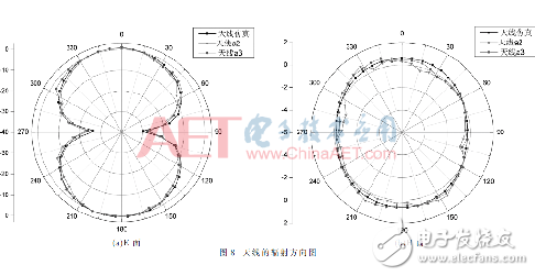
The radiation patterns of antenna a2 and antenna a3 are tested, and the results are shown in Figure 8. The radiation patterns of antenna a2 and antenna a3 are basically consistent with the simulation results. Figure 8(a) shows that the antenna has bidirectional radiation characteristics on the E surface, and Figure 8(b) shows that the antenna has good omnidirectional radiation on the H surface. Generally speaking, the radiation of antenna a2 and antenna a3 is relatively stable, and the performance is good. To sum up, the antenna a3 made by the pattern inversion process based on AZ5214E ​​glue has the best performance in the experiment. It can be seen that the metal gap and signal conduction band of its CPW structure have the highest precision, the least difficulty in processing and peeling, and have a high success rate; it is made based on RZJ304 glue. The performance of the antenna a2 is better, the precision of the CPW gap and the signal conduction band is high, the processing and peeling is difficult, and the success rate is low; and it is difficult to peel off the AZ6130 glue to make a CPW antenna that meets the requirements, and the gap of the CPW structure is difficult to achieve. Completely peels off clean.
4 Conclusion
In this paper, a small ultra-wideband coplanar waveguide structure-fed MEMS monopole flexible antenna is proposed, which uses PDMS material with high flexibility and good self-recovery as the dielectric substrate, and one side of the PDMS flexible substrate is used. Nickel-coated, and fed by a CPW that can be integrated on the same side of the flexible substrate as the disc-shaped radiating metal structure of the antenna. In order to reduce the influence of the dimensional processing error of the CPW structure on the performance of the antenna, the method of fabricating fine structures based on the metal stripping process on the PDMS flexible substrate was explored. antenna. The experiment found that the CPW-fed flexible antenna based on the pattern inversion process of AZ5214E ​​glue has the best performance. It can be seen that the metal gap and signal conduction band of the CPW structure have the highest accuracy, the lowest peeling difficulty and high success rate. The combined treatment of PDMS by oxygen plasma etching and SDS can effectively improve the adhesion between photoresist and PDMS surface. The frequency band of the antenna is 3.3 GHz to 5.0 GHz, the impedance matching is good, and the radiation direction is stable.
Uv Curving Glass,Tempered Glass Screen Protector,Film Cutting Machine,Uv Curing Protector Screen
Shenzhen TUOLI Electronic Technology Co., Ltd. , https://www.hydrogelprotectors.com