To help the growing design team, the EDA industry must provide designers with automated solutions that enable the entire process to execute smoothly. These solutions must optimize power while meeting all other design and market requirements, including speed, cost, and IC manufacturing yield.
Power problem overview
By making trade-offs at the system level and making relevant decisions, the power and energy consumption of consumer devices can be minimized. Decisions about system partitioning (ie, determining which functionality is implemented by hardware or software), components, and IP selection have the greatest impact on power and system performance and functionality.
E.g. In a hard disk-based MP3 player, one of the key architectural features for power management is the software control data buffering system, which allows the hard disk to provide music equivalent to a few minutes each time, then stop spinning and wait for the next One time music. Although many mobile phones are now highly optimized for voice communication at the architectural level, pressure from consumers has forced designers to add a host of other features from email to streaming video to MP3 players.
As a result, system designers have to use more and more aggressive architectures to manage power. To support this effort, the EDA industry continues to improve its system-level power modeling tools to provide system designers with feedback on the impact of their architectural decisions.
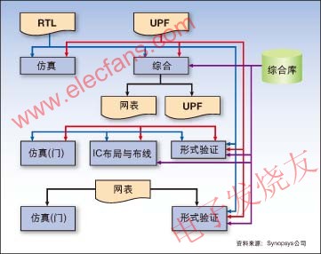
Figure: Collaborate with golden RTL in the design to systematically use UPF to reduce dynamic and static power consumption throughout the design flow through DVFS and power gating techniques.
Hardware power management technology
Once the system architecture is determined and the main application ICs are selected, various hardware power management techniques can be applied.
RTL designers can take advantage of technologies such as clock gating, logic and cell-level power optimization, and multi-threaded voltage design as part of a standard, integrated design process. Automated application of these technologies reduces power consumption while maintaining performance, testability, and manufacturability. But this requires a library of integrated clock gating cells and logic cells to provide multiple drive forces and multiple threshold levels, as well as tools to use the functions of these cell libraries. Today's EDA tools have such capabilities, and the use of these technologies is becoming more common. More radical power management methods are still at the forefront of design principles and EDA tool capabilities.
Dynamic power is proportional to V2, so to minimize dynamic power, the key is to reduce the supply voltage. Designers have begun to use on-chip multi-voltage domains: higher voltage domains for high-performance modules such as processors and buffers; lower voltage domains for other modules with lower operating frequencies. This solution requires the insertion of a level shifter between modules with different operating voltages. This bold design is based on the workload of the main components (such as the processor), dynamically assigning them the supply voltage and clock frequency, known as Dynamic Voltage and Frequency Modulation (DVFS).
As process geometries continue to shrink to 90 nanometers, 65 nanometers and below, leakage current issues are becoming more prominent, limiting the battery life of handheld devices. To minimize leakage power, designers began using power gating—turning off the power to the unused modules, usually with an on-chip switch. Thus, isolation cells are required between domains that are powered down and powered up, and a strategy is needed to preserve the state during the shutdown.
These techniques are extremely effective for consumer applications that have peak processing requirements (such as video encoding/decoding) but have plenty of time to idle. With an adaptive power management scheme, designers can maximize the performance of the designed chip while operating in ultra-low power mode when the workload of some modules in the design is reduced.
With proper hardware design and other factors, DVFS and power gating technology can be controlled by software to achieve significant energy savings and extend battery life.
These adaptive technologies require smarter design automation techniques and more flexible IP. Designers need a way to specify power intent, which is to determine which domain is powered by which domain, which domain can be turned off, and when to use what strategy to preserve the state during the shutdown. Designers generally expect this determination of design intent to be independent of RTL because a particular RTL module may have different power intents in different applications.
Therefore, the implementation tool needs to set the power intent and insert the level shifter, isolation unit, and holding registers in the appropriate locations and route the power correctly to all devices in the chip. In particular, these tools require proper buffering of the signal, i.e., when the signal is needed, the buffer is powered up and turned off when not needed. Some of these routing rules can become quite complex.
The sign-off tool must now contain voltage-dependent timing and power grid integrity. Validation (regular and dynamic) must be able to handle changes in design behavior resulting from increased power gating techniques. IP vendors must also assist in the development of a wider range of low-power IPs, including level shifters, isolation units, hold triggers, and power gating switches. In order to support DVFS, the cell library must also be characterized for large voltage ranges, not just one or two special operating points.
Unified power format
Fortunately, mainstream industry companies have joined forces to introduce low-power solutions that integrate more automated EDA tools, more flexible IP, standard formats, and more demanding process technologies into true end-to-end solutions. . Recently, a large number of leading semiconductor, EDA and IP companies within the Accellera standards organization are actively developing a unified power format (UPF). The UPF provides a mechanism to describe the power intent of an RTL-independent design. It allows designers to define the power domain, isolation strategy, and retention strategy required for power gating. It also allows designers to define level shifter strategies and power state tables to handle multiple power domains. With UPF, all tools in the full design flow can be unified to implement and validate the same set of power reduction strategies.
In collaboration with golden RTL in the design, UF is systematically used in the full design flow to reduce dynamic and static power through DVFS and power gating techniques.
Liquid Crystal Display For Instrument
Liquid Crystal Display For Instrument,Large Industrial Precision Lcd Display,Small Industrial Body Thin Lcd Display,Precise Liquid Crystal Display
Dongguan Yijia Optoelectronics Co., Ltd. , https://www.everbestlcdlcms.com