From 2 inches, 3 inches, 4 inches to today's 6-inch silicon carbide single crystal substrate, Chen Xiaolong team spent more than 10 years, the first in China to achieve independent research and development and industrialization of silicon carbide single crystal substrate.
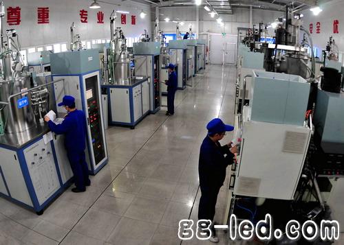
Not long ago, researcher Chen Xiaolong of the Institute of Physics of the Chinese Academy of Sciences cooperated with Beijing Tianke Heda Blu-ray Semiconductor Co., Ltd. (hereinafter referred to as Tianke Heda) to solve the 6-inch diameter expansion technology and wafer processing technology, and successfully developed 6 inches. Silicon carbide single crystal substrate.
From 2 inches, 3 inches, 4 inches to today's 6-inch silicon carbide single crystal substrate, Chen Xiaolong team spent more than 10 years, the first in China to achieve independent research and development and industrialization of silicon carbide single crystal substrate.
The third-generation semiconductor materials <br> <br> researchers told reporters, the fifties and sixties, silicon and germanium form the first generation of semiconductor materials, mainly used in low-voltage, low-frequency, medium power transistors and photodetectors. Compared with germanium semiconductor devices, semiconductor devices fabricated from silicon materials have better high temperature and radiation resistance.
By the late 1960s, more than 95% of semiconductors and 99% of integrated circuits were fabricated from silicon semiconductor materials. Until now, most of the semiconductor products we use are based on silicon materials.
After entering the 1990s, gallium arsenide and indium phosphide represent the second generation of semiconductor materials that can be used to make high-speed, high-frequency, high-power, and light-emitting electronic devices. Due to the rise of information highways and the Internet, second-generation semiconductor materials are widely used in satellite communications, mobile communications, optical communications, and GPS navigation.
Compared to the first two generations of semiconductor materials, third-generation semiconductor materials are often referred to as wide-bandgap semiconductor materials or high-temperature semiconductor materials. Among them, silicon carbide and gallium nitride are well-established representatives in the third generation of semiconductor materials.
The reporter learned that silicon carbide single crystal is a wide bandgap semiconductor material with many forbidden band width, strong critical breakdown field, high thermal conductivity and high saturation drift speed. It is widely used in high temperature and high frequency. And high power electronics.
Regarding gallium nitride, it has been reported that a 2-inch GaN wafer can produce 10,000 ç› brightness for energy-saving lamps 10 times, luminous efficiency for energy-saving lamps 3-4 times, and life expectancy 10 times higher than energy-saving lamps. Brightness LED lighting; 5,000 blue lasers with an average price of around $100 can also be manufactured; they can also be used in power electronics to reduce system energy consumption by more than 30%.
Due to the small lattice mismatch between silicon carbide and gallium nitride, silicon carbide single crystal is an ideal substrate material for devices such as gallium nitride-based LEDs, Schottky diodes, and gold oxide half field effect transistors. The Chen Xiaolong Research Group (Functional Crystal Research and Application Center) of the Advanced Materials and Structure Analysis Laboratory of the Institute of Physics has long been engaged in the research of silicon carbide single crystal growth.
To this end, researchers grow gallium nitride thick films on other substrates (such as silicon carbide), and then separate the substrate and gallium nitride thick film by stripping technology. The separated gallium nitride thick film can be used as epitaxial. Substrate. Despite the epitaxy of a gallium nitride thick film as a substrate, the bit error density is significantly lower than that of a gallium nitride film epitaxially grown on a silicon carbide material, but it is expensive.
Therefore, the Chen Xiaolong team chose the silicon carbide single crystal substrate research. He pointed out that silicon carbide single crystal substrates have many outstanding advantages, such as good chemical stability, good electrical conductivity, good thermal conductivity, and no absorption of visible light, but they are also insufficient, such as the price is too high.
In the early years, the price of silicon carbide wafers in the global market was very expensive. The international market price of a 2-inch silicon carbide wafer was as high as $500 (2006), but it is still in short supply. High raw material costs account for more than 10% of the price of silicon carbide semiconductor devices. "The price of silicon carbide wafers has become the bottleneck for the development of the third-generation semiconductor industry." Chen Xiaolong said.
In order to reduce the cost of the device, the downstream industry has put forward a large size requirement for the silicon carbide single crystal substrate. Therefore, the use of advanced silicon carbide crystal growth technology to achieve large-scale production, reduce the cost of silicon carbide wafer production, will promote the rapid development of the third-generation semiconductor industry, expand market demand.
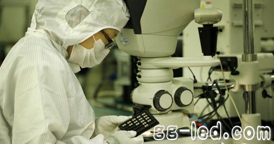
Tianke Heda was established in 2006, relying on the research results of the research and development team in the field of silicon carbide in Chen Xiaolong's research team. Since its inception, Tianke Heda has developed a silicon carbide crystal growth furnace and silicon carbide crystal growth, processing technology and professional equipment, and established a complete silicon carbide wafer production line.
Over the years, Tianke Heda has been committed to improving the quality of silicon carbide crystals and the development of large-size silicon carbide crystals, industrializing advanced silicon carbide crystal growth and processing technologies, and mass production and sales of silicon carbide with independent intellectual property rights. Wafer.
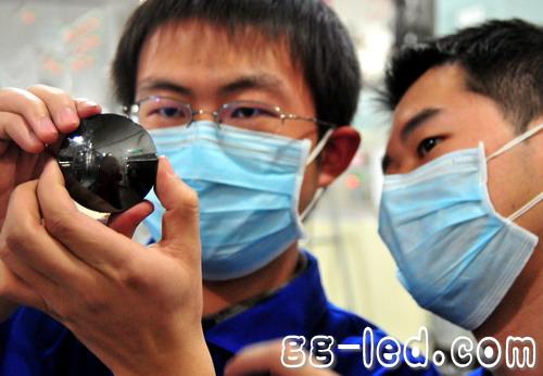
In 2013, the Chen Xiaolong team began research and development of 6-inch silicon carbide crystals. In the past year, the domestically produced 6-inch silicon carbide single crystal substrate was developed. The test proves that the crystal quality of the domestic 6-inch silicon carbide crystal is very good. The result indicates that the research and development of the silicon carbide single crystal in the physical field has reached the international advanced level and can provide a material basis for the localization of high-performance silicon carbide-based electronic devices.
"Although it started a bit late, but through more than 10 years of independent research and development, the gap between our technology and foreign technology is gradually narrowing." Chen Xiaolong said. As a pioneer in the production and manufacture of domestic silicon carbide wafers, Tianke Heda broke the foreign monopoly and filled the domestic gap. The silicon carbide wafers produced are not only mature in technology, but also lower than the prices of similar international products.
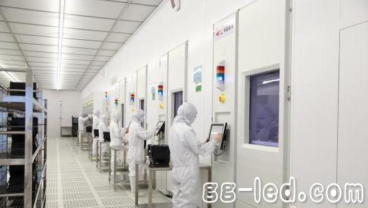
As of March 2014, Tianke Heda has formed a production line with an annual output of 70,000 silicon carbide wafers, which has promoted the sustained and stable development of China's third-generation semiconductor industry and achieved good economic and social benefits.
Chen Xiaolong pointed out that the current silicon carbide is mainly used in three major areas: high-brightness LED, power electronics and advanced radar. It may enter the home market in the future, which means that the independent innovation and industrialization of the Chen Xiaolong team will continue.

Not long ago, researcher Chen Xiaolong of the Institute of Physics of the Chinese Academy of Sciences cooperated with Beijing Tianke Heda Blu-ray Semiconductor Co., Ltd. (hereinafter referred to as Tianke Heda) to solve the 6-inch diameter expansion technology and wafer processing technology, and successfully developed 6 inches. Silicon carbide single crystal substrate.
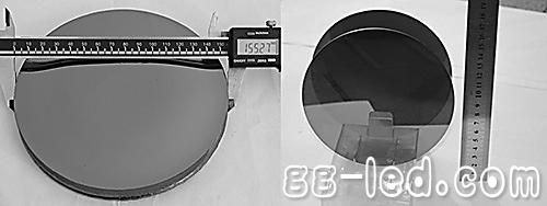
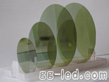
Data sheet: 6-inch silicon carbide crystal and single crystal substrate
From 2 inches, 3 inches, 4 inches to today's 6-inch silicon carbide single crystal substrate, Chen Xiaolong team spent more than 10 years, the first in China to achieve independent research and development and industrialization of silicon carbide single crystal substrate.
The third-generation semiconductor materials <br> <br> researchers told reporters, the fifties and sixties, silicon and germanium form the first generation of semiconductor materials, mainly used in low-voltage, low-frequency, medium power transistors and photodetectors. Compared with germanium semiconductor devices, semiconductor devices fabricated from silicon materials have better high temperature and radiation resistance.
By the late 1960s, more than 95% of semiconductors and 99% of integrated circuits were fabricated from silicon semiconductor materials. Until now, most of the semiconductor products we use are based on silicon materials.
After entering the 1990s, gallium arsenide and indium phosphide represent the second generation of semiconductor materials that can be used to make high-speed, high-frequency, high-power, and light-emitting electronic devices. Due to the rise of information highways and the Internet, second-generation semiconductor materials are widely used in satellite communications, mobile communications, optical communications, and GPS navigation.
Compared to the first two generations of semiconductor materials, third-generation semiconductor materials are often referred to as wide-bandgap semiconductor materials or high-temperature semiconductor materials. Among them, silicon carbide and gallium nitride are well-established representatives in the third generation of semiconductor materials.
The reporter learned that silicon carbide single crystal is a wide bandgap semiconductor material with many forbidden band width, strong critical breakdown field, high thermal conductivity and high saturation drift speed. It is widely used in high temperature and high frequency. And high power electronics.
Regarding gallium nitride, it has been reported that a 2-inch GaN wafer can produce 10,000 ç› brightness for energy-saving lamps 10 times, luminous efficiency for energy-saving lamps 3-4 times, and life expectancy 10 times higher than energy-saving lamps. Brightness LED lighting; 5,000 blue lasers with an average price of around $100 can also be manufactured; they can also be used in power electronics to reduce system energy consumption by more than 30%.
Due to the small lattice mismatch between silicon carbide and gallium nitride, silicon carbide single crystal is an ideal substrate material for devices such as gallium nitride-based LEDs, Schottky diodes, and gold oxide half field effect transistors. The Chen Xiaolong Research Group (Functional Crystal Research and Application Center) of the Advanced Materials and Structure Analysis Laboratory of the Institute of Physics has long been engaged in the research of silicon carbide single crystal growth.
To this end, researchers grow gallium nitride thick films on other substrates (such as silicon carbide), and then separate the substrate and gallium nitride thick film by stripping technology. The separated gallium nitride thick film can be used as epitaxial. Substrate. Despite the epitaxy of a gallium nitride thick film as a substrate, the bit error density is significantly lower than that of a gallium nitride film epitaxially grown on a silicon carbide material, but it is expensive.
Therefore, the Chen Xiaolong team chose the silicon carbide single crystal substrate research. He pointed out that silicon carbide single crystal substrates have many outstanding advantages, such as good chemical stability, good electrical conductivity, good thermal conductivity, and no absorption of visible light, but they are also insufficient, such as the price is too high.
In the early years, the price of silicon carbide wafers in the global market was very expensive. The international market price of a 2-inch silicon carbide wafer was as high as $500 (2006), but it is still in short supply. High raw material costs account for more than 10% of the price of silicon carbide semiconductor devices. "The price of silicon carbide wafers has become the bottleneck for the development of the third-generation semiconductor industry." Chen Xiaolong said.
In order to reduce the cost of the device, the downstream industry has put forward a large size requirement for the silicon carbide single crystal substrate. Therefore, the use of advanced silicon carbide crystal growth technology to achieve large-scale production, reduce the cost of silicon carbide wafer production, will promote the rapid development of the third-generation semiconductor industry, expand market demand.
Tianke Heda was established in 2006, relying on the research results of the research and development team in the field of silicon carbide in Chen Xiaolong's research team. Since its inception, Tianke Heda has developed a silicon carbide crystal growth furnace and silicon carbide crystal growth, processing technology and professional equipment, and established a complete silicon carbide wafer production line.
Over the years, Tianke Heda has been committed to improving the quality of silicon carbide crystals and the development of large-size silicon carbide crystals, industrializing advanced silicon carbide crystal growth and processing technologies, and mass production and sales of silicon carbide with independent intellectual property rights. Wafer.
In 2013, the Chen Xiaolong team began research and development of 6-inch silicon carbide crystals. In the past year, the domestically produced 6-inch silicon carbide single crystal substrate was developed. The test proves that the crystal quality of the domestic 6-inch silicon carbide crystal is very good. The result indicates that the research and development of the silicon carbide single crystal in the physical field has reached the international advanced level and can provide a material basis for the localization of high-performance silicon carbide-based electronic devices.
"Although it started a bit late, but through more than 10 years of independent research and development, the gap between our technology and foreign technology is gradually narrowing." Chen Xiaolong said. As a pioneer in the production and manufacture of domestic silicon carbide wafers, Tianke Heda broke the foreign monopoly and filled the domestic gap. The silicon carbide wafers produced are not only mature in technology, but also lower than the prices of similar international products.
As of March 2014, Tianke Heda has formed a production line with an annual output of 70,000 silicon carbide wafers, which has promoted the sustained and stable development of China's third-generation semiconductor industry and achieved good economic and social benefits.
Chen Xiaolong pointed out that the current silicon carbide is mainly used in three major areas: high-brightness LED, power electronics and advanced radar. It may enter the home market in the future, which means that the independent innovation and industrialization of the Chen Xiaolong team will continue.
Yixing Futao Metal Structural Unit Co. Ltd. is com manded of Jiangsu Futao Group.
It is located in the beach of scenic and rich Taihu Yixing with good transport service.
The company is well equipped with advanced manufacturing facilities.
We own a large-sized numerical control hydraulic pressure folding machine with once folding length 16,000mm and the thickness 2-25mm.
We also equipped with a series of numerical control conveyor systems of flattening, cutting, folding and auto-welding, we could manufacture all kinds of steel poles and steel towers.
Our main products: high & medium mast lighting, road lighting, power poles, sight lamps, courtyard lamps, lawn lamps, traffic signal poles, monitor poles, microwave communication poles, etc. Our manufacturing process has been ISO9001 certified and we were honored with the title of the AAA grade certificate of goodwill.
Presently 95% of our products are far exported to Europe, America, Middle East, and Southeast Asia, and have enjoyed great reputation from our customers.
So we know the demand of different countries and different customers.
We are greatly honored to invite you to visit our factory and cheerfully look forward to cooperating with you.
Single Arm Type Pole,Single Arm Type Street Pole,Single Arm Type Light Pole
YIXING FUTAO METAL STRUCTURAL UNIT CO.,LTD( YIXING HONGSHENGYUAN ELECTRIC POWER FACILITIES CO.,LTD.) , https://www.chinasteelpole.com