The characteristics of the 1 555 time base circuit 555 integrated circuit is used as a timer application, so it is called 555 timer or 555 time base circuit. However, after development, in addition to timing delay control, it can also be used for dimming, temperature regulation, pressure regulation, speed regulation and other various control and measurement detection. In addition, it can also constitute pulse oscillation, monostable, bistable and pulse modulation circuits for AC signal source, power conversion, frequency conversion, pulse modulation and so on. Because it is reliable, easy to use, and inexpensive, it is widely used in various electronic products. There are dozens of components inside the 555 integrated circuit, including voltage dividers, comparators, basic RS flip-flops, discharge tubes, and buffers. The circuit is more complicated, and it is a mixture of analog circuit and digital circuit, as shown in Figure 1. 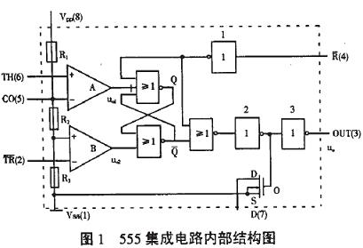
Figure 1 555 integrated circuit internal structure diagram 555 integrated circuit is 8-pin package, dual in-line type, as shown in Figure 2 (A), according to the input and output arrangement can be seen as shown in Figure 2 (B). The 6-pin is called the threshold end (TH), which is the input of the upper comparator; the 2-pin is called the trigger end (TR), which is the input of the lower comparator; the 3-pin is the output end (Vo), which has two states of O and 1. It is determined by the level applied by the input terminal; 7 pin is the discharge end (DIS), which is the output of the internal discharge tube. It has two states of floating and grounding, which is also determined by the state of the input terminal; 4 is the reset end (MR) ), when the low level is added, the output can be low level; the 5 pin is the control voltage terminal (Vc), which can be used to change the upper and lower trigger level values; 8 feet are the power supply end, and 1 pin is the ground end. 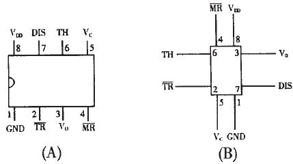
Figure 2 555 integrated circuit package diagram We can also equivalent 555 circuit into a RS flip-flop with discharge switch, as shown in Figure 3 (A), this special trigger has two inputs: threshold end (TH) Can be seen as the zero terminal R, requires a high level, the trigger terminal (TR) can be seen as the set terminal S, requires a low level, there is an output terminal Vo, Vo can be equivalent to the Q end of the trigger, The discharge end (DIS) can be regarded as a contact controlled by the internal discharge switch, controlled by the Q terminal of the trigger: when the Q=1, the DIS terminal is grounded, and when Q=0, the DIS terminal is suspended. There is also a reset terminal MR, a control voltage terminal Vc, a power supply terminal VDD and a ground terminal GND. This special trigger has two features:
(1) The trigger level of the two inputs requires one high and one low, the zero terminal R, that is, the threshold terminal (TH) requires a high level, and the set terminal s, that is, the trigger terminal (TR), requires low power;
(2) The threshold voltage values ​​of the two input terminals cause the output to be inverted. When the V c terminal is not connected to the control voltage, >2/3VDD is high level 1 for the TH(R) terminal. <2/3VDD is a low level 0: for the TR(S) terminal, >1/3VDD is a high level 1, and <1/3VDD is a low level 0. If the voltage Vc is controlled on the control terminal (Vc), then the upper trigger level becomes the Vc value, and the lower trigger level becomes the 1/2Vc value. It can be seen that changing the control voltage value of the control terminal can change the upper and lower trigger voltages. Flat value. Its function table is shown in Figure 3 (B).
This article refers to the address: http://
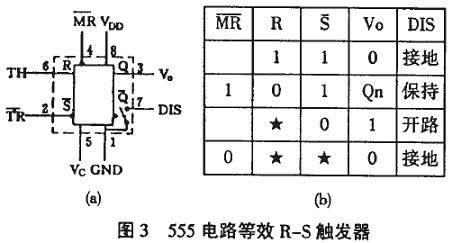
Figure 3 555 circuit equivalent R-S flip-flop 555 integrated circuit has two types of bipolar and CMOS. The advantages of the CMOS type are low power consumption, low power supply voltage, high input impedance, but low output power, and the output drive current is only a few milliamperes. The advantage of the bipolar type is that the output power is large, the drive current is up to 200 mA, and other indicators are not as good as the CMOS type.
There are many application circuits of 555. As long as the external additional circuit of 555 integrated circuit is changed, hundreds of application circuits can be formed, which can be roughly divided into three categories: 555 monostable, 555 bistable and 555 unsteady (or oscillator).
The 2 555 monostable circuit monostable circuit has a steady state and a temporary steady state. It uses the charge and discharge of the capacitor to form a transient state. Therefore, its input terminal has a timing resistor and a timing capacitor. The common 555 monostable circuit There are two types:
1) The manual start type connects the 6 and 2 pins of the 555 circuit to the RC timing circuit. In the timing capacitor CT, the push button switch SB is connected at both ends, which becomes the manual start type 555 one-shot circuit, as shown in Fig. 4 (a ), replacing the 555 with an equivalent trigger and omitting the part unrelated to the one-shot operation is shown in Figure 4(b). The following is how it works:
Steady state: After the power is connected, the capacitor CT is quickly charged to VDD. As seen in Figure 4(b), the trigger input R=1, S=1, and the output Vo=0 is seen from the function table. This is its Steady state.
Temporary steady state: When the switch SB is pressed, the charge on the CT is quickly placed to zero, which is equivalent to the trigger input R=0, S=0, and the output is immediately turned into Vo=l, and the transient steady state starts. After the switch is released, the power supply is charged to the CT again. After the time TD, when the voltage on the CT rises to >2/3VDD, the output is turned over to Vo=O, and the transient steady state ends. TD is the timing time or delay time of the one-shot circuit, which is related to the values ​​of the timing resistor RT and the timing capacitor CT: TD=1.1RTCT. 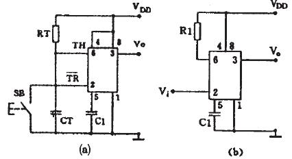
Figure 4 Manually activated 555 single-stable circuit 2) Pulse-start type Connect the 6 and 7 pins of the 555 circuit together on the timing capacitor CT, and use the 2-pin input to become the pulse-starting monostable circuit, as shown in Figure 5 ( a), the 2 feet of the circuit are normally connected to the high level. When the input is connected to the low level or the negative pulse is input, the circuit is started. After replacing the 555 with the equivalent flip-flop, as shown in Figure 5 6), analyze it below. working principle:
Steady state: After the power is connected, R=1, S=1, the output Vo=0, the DIS terminal is grounded, the voltage on the CT is 0, that is, R=0, and the output remains Vo=0, which is its steady state.
Temporary steady state: After inputting negative pulse, input S=0, the output immediately flips to Vo=1, the DIS end is open, the power supply is charged to the CT through RT, and the transient steady state begins. After the elapse of time TD, when the voltage on the CT rises to >2/3VDD, the input becomes R=1 and S=1. At this time, the negative pulse has disappeared, and the output is inverted to Vo=0, and the transient steady state ends. At this time, the internal discharge switch is turned on, the DIS terminal is grounded, and the charge on the CT is quickly placed to zero to prepare for the next timing control. The timing time of the circuit is TD=1.1RTCT.
These two one-shot circuits are often used as timing delay controls. 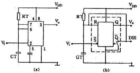
Figure 5 pulse-starting monostable circuit
There are two common 555 bistable circuits for the 3 555 bistable circuit:
1) RS flip-flop type bistable uses the 6 and 2 pins of the 555 circuit as two control inputs. When the 7-end is not used, it becomes an RS flip-flop. Note that the trigger level of the two inputs is different from the threshold voltage. As shown in Figure 6(a), there may be only one control terminal. At this time, another control terminal should try to connect to the dead end. According to the circuit requirements, the R terminal can be connected to the power supply terminal. As shown in Fig. 6(b), it is also possible to ground S and use the R terminal as an input.
A bistable circuit with two inputs is often used for motor speed regulation, power supply upper and lower limit alarms, and the like. A bistable circuit with an input is used as a single-ended comparator for various detection circuits. 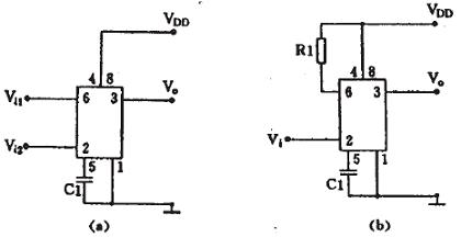
Figure 6 555 constitutes the RS flip-flop 2) Schmitt trigger type bistable connects the 6 and 2 pins of the 555 circuit together to form a trigger with only one input, as shown in Figure 7(a), this trigger output The relationship between the voltage and the input voltage is a rectangular return line shape. As shown in Fig. 7(b), it can be seen from the curve that when the input V1=0, the output Vo=1, when the input voltage rises from 0 to >2/3VDD, Vo flips to 0, and Vo drops to 1 again when the input voltage drops from the highest value to <1/3VDD. Since its input has two different threshold voltages, this circuit is often used for electronic switches, various control circuits, waveform transformations and shaping, as shown in Figure 8.
Figure 7 555 constitutes a Schmitt trigger 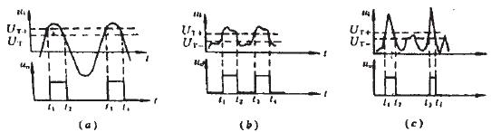
Figure 8 waveform transformation and shaping
4 555 unstable circuit (oscillator)
The multivibrator composed of the 555 timer is shown in Fig. 9(a), and its operating waveform is shown in Fig. 9(b).
After the power is turned on, the power supply VDD charges the capacitor C through R1 and R2. When Uc < 1/3VDD, the oscillator output Vo=1, and the discharge tube is turned off. When Uc is charged to ≥2/3VDD, the oscillator output Vo is turned to 0. At this time, the discharge tube is turned on, the discharge terminal (DIS) is grounded, and the capacitor C is discharged to the ground through R2, causing Uc to drop. When Uc drops to ≤ 1/3VDD, the oscillator output Vo is flipped again to 1, and the discharge tube is turned off again, so that the discharge terminal (DIS) is not grounded, and the power supply VDD charges the capacitor C through R1 and R2 again, and makes Uc As it rises from 1/3VDD to 2/3VDD, the flip-flop flips again, and so on, so that a continuously varying oscillating pulse waveform is obtained at the output Vo. The pulse width TL ≈ 0.7R2C is determined by the discharge time of the capacitor C; TH = 0.7 (R1 + R2) C, which is determined by the charging time of the capacitor C, and the pulse period T ≈ TH + TL. 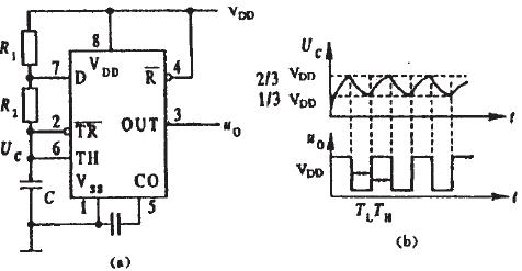
Figure 9 555 constitutes a multivibrator. Only a few typical application examples consisting of 555 timers are discussed above. In fact, because the 555 timer has high sensitivity and flexible functions, it is widely used in electronic circuits.
Fertilizer Granulator Machine,fertilizer extruding machine,Organic fertilizer granulating machine
Dry Roll Press Granulator Co., Ltd. , http://www.nspelletmill.com