1 Introduction
Wireless sensor networks (WSNs), which integrate sensor technology, embedded computing technology, wireless network communication technology, distributed information processing technology and micro-electromechanical technology, are currently a hot research topic. The wireless sensor network can realize complex monitoring and tracking tasks in a wide range of application fields. It is a wireless network composed of randomly distributed integrated sensors, data processing units and communication micro-nodes in a self-organized manner. The wireless sensor network node generally includes a sensing unit, an embedded processing unit, a wireless communication unit, a power supply self-powered system, and a positioning system. As a special type of ad hoc, in addition to dynamic topology, self-organization, multi-hop routing, limited bandwidth, etc., it also has an extremely remarkable feature: energy limitation. Therefore, network nodes have the characteristics of low power consumption, low cost and small size.
With the rapid development of IC manufacturing processes, system-on-chip (SOC) has been widely used. SOC closely integrates the system's processing mechanism, model algorithm, chip structure, design of circuits and devices at various levels, and completes the entire system on one chip. Compared with the traditional multi-IC electronic system, it has the following advantages: low power consumption and high reliability (reducing the number of external pins of the chip, reducing the signal transmission between the peripheral drive interface unit and the circuit board, the embedded circuit can Avoid system interference), high integration.
This paper presents a SOC solution for wireless sensor network nodes, analyzes the architecture of wireless sensor network nodes, and explains the wireless sensor network node chip from the aspects of system level, structural level, RTL level and physical design. Low power consumption design.
2. SOC system on chip and VLSI low power consumption
With the rapid development of IC manufacturing processes, system-on-chip (SOC) has been widely used. SOC closely integrates the system's processing mechanism, model algorithm, chip structure, design of circuits and devices at various levels, and completes the entire complex system in one piece. Compared with the traditional multi-IC electronic system, it has the following advantages: low power consumption and reliability (reducing the number of external pins of the chip, reducing the signal transmission between the peripheral drive interface unit and the circuit board, and the embedded circuit can be avoided System interference), high integration, less development cost, and shorter development cycle.
VLSI low-power design and optimization is a very complex issue, generally considered from the following stages:
1. System design stage. At this stage, we must consider the coordinated design and synthesis of software and hardware. On the basis of implementing application functions, it is necessary to select which functions are implemented by hardware and which operations with large power consumption are performed by software. At the same time, in system design, we must also consider the power mode of the hardware itself: design sleep mode and wake-up operation. At the same time, it adopts power consumption management strategy and variable voltage technology.
2. Structural level. The use of bus coding technology mainly reduces power consumption by reducing flip activity. Adopt the parallel structure, while the performance is replaced with the area, the working frequency can be reduced to reduce power consumption. Using a pipeline structure, this method is actually a special case of retiming (reTIming). By shortening the critical path and reducing the value of the capacitor on the path, the power consumption is reduced. Other ReTIming (retiming) and Unfolding (expansion) can also reduce power consumption at the algorithm level.
3. RTL level. Mainly reduce power consumption by adopting a low-power comprehensive process. At this stage, a gating clock will be added to reduce the dynamic flip rate.
4. Physical design. Adopt multi-power multi-threshold voltage cell library, and low-power physical design process and EDA software. Design multiple power domains and optimize dynamic power consumption to reduce power consumption. When synthesizing the clock tree, while balancing the skew, try to insert the driver at the node with the lower flip rate.
3. Low-power design at the system level
From the perspective of the coordination of software and hardware, the node structure of the designed wireless sensor network is shown in Figure 1. The whole system coordinates the communication and work of each sub-module through the core unit RISC CPU core. The TRF6903 chip is a multi-band RF RF transceiver chip with low power consumption and low voltage. It supports 315/433/868/915 Mhz optional frequency band, supports frequency hopping protocol, and internally completes FSK / OOK modulation with a speed of up to 64kbps. The characteristics of TRF6903's low power consumption make it suitable for battery power supply, which is consistent with the low power consumption requirements of network nodes.
The baseband processing unit module is used to realize the functions of the physical layer and part of the data link layer based on the IEEE 802.15.4 protocol; the upper layer protocol of the data link layer can be implemented by software to save power consumption. This is because if the complex network layer, transport layer, and application layer are implemented in hardware, although the speed will increase, the complexity of the hardware will also increase, which will inevitably bring about an increase in power consumption.
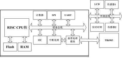
Figure 1 SOC design block diagram of wireless sensor network node
At the system level, the RISC CPU core has designed idle mode and stop mode to save power consumption. When the RISC CPU core enters idle mode or stop mode, the CPU's internal clock stops running, while the internal registers hold data.
4. Low-power design at the structural level
Through careful analysis of the power consumption sources of the entire SOC chip, it can be seen that the RISC CPU core, RAM, Flash and baseband processing modules account for the vast majority. The low-power design is carried out from the structural level.
4.1 Low-power design of RISC CPU core
The reduction of the power consumption of the microprocessor can be solved by reducing the frequency and reducing the working voltage. In the design of the network node SOC structure level, in addition to the slow clock and low voltage power supply methods, it is also optimized for the data path at the same time, the main purpose is to reduce unnecessary flips in the circuit. Optimization of instruction decoding data path: In general, all execution units in the CPU are directly connected to the instruction decoding unit. Once there is new decoded data input, all the execution unit circuits connected to it will also be flipped, resulting in unnecessary waste of power consumption. Therefore, without affecting the timing function, a separate internal bus is designed, and the input data and control signals of the unit that are not executed are latched, the input signals remain unchanged, and the dynamic power consumption can be reduced. RAM and Flash ROM are integrated inside the chip. In order to reduce the power consumption of these two and avoid unnecessary flipping, the interface unit of the internal bus and RAM, Flash design latch, in this way, only when the CPU accesses the corresponding address, RAM and Flash internal flip.
4.2 Low-power design of baseband processing module
The design block diagram of the baseband processing module is shown in Figure 2; its physical layer frame and data link layer frame structure based on IEEE 802.15.4 protocol are shown in Figure 3. From the perspective of improving CPU efficiency and reducing power consumption, the baseband processing module communicates with the CPU by using an interrupt method. The baseband processing module finishes sending the data frame of the receiving FIFO, applies to the CPU for sending an interrupt, and waits for the CPU to write new data to the sending FIFO; when the baseband processing module receives the data frame sent by the TR6903 module, it stores it in the receiving FIFO and generates a reception The interrupt waits for the CPU to process.
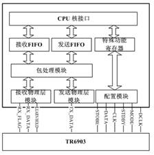
Figure 2 Block diagram of the baseband processing module
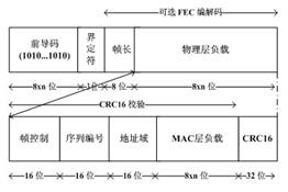
Figure 3 Physical layer and data link layer frame structure
The baseband processing module mainly uses parallel structure and pipeline technology to reduce power consumption. The physical layer sending module of the sending function and the receiving function, the buffer are all parallel structures. The configuration modules are also designed separately, and the data processing methods are also parallel. The CRC16 in the packet processing module is also checked using a parallel structure. The advantage of this design is to improve performance through parallel design at a slow clock frequency and achieve the same performance as high-speed hourly speed. There is a pipeline stage between each sub-module and sub-module in Figure 2, which is not only to reduce unnecessary flips, but also to reduce the length of the critical path more importantly, so as to achieve indirect reduction purpose.
The low-power structure design of the baseband processing module is as follows:
ï¬
Send FIFO, receive FIFO: for receiving, sending frame buffer, used to store the MAC layer data load.
ï¬
SFR special function register: 1, interrupt register. There are mainly send and receive interrupt flags, interrupt enable bits, FIFO overflow flag bits, send and receive start bits. 2. Configuration register. The CPU selects the working mode and working rate of TR6903 by writing to the SFR register. 3. Status register: store the number of data bytes of FIFO, etc.
ï¬
Packet processing module: use hardware to implement some functions of the data link layer. In the transmission mode, add variable byte preamble, 3-bit delimiter, 1 byte frame length, optional forward error correction coding, 2 bytes CRC16 check these data as MAC layer load; In the receiving mode, the packet processing module completes the unpacking of the data packet. The main work is the detection of the preamble, the detection of the delimiter, the optional 1 byte address comparison, and the 2 byte CRC16 check.
ï¬
Configuration module: configure the control module to control the timing of the CLK, DATA, STOBE pins according to the corresponding configuration in SFR to control the corresponding state of TR6903, and realize the function of frequency hopping.
Receiving physical layer module: receiving control module to realize the function of physical layer sending data. After the RX_FLAG signal is high, that is, after detecting the delimiter, the state of the RX_DATA pin is sampled at the rising edge of DCLK, and the frame length byte, the physical layer payload, and the 2 byte CRC16 check are received in turn to the packet processing module Processing, and at the same time output the corresponding high level from the LEARN / HOLD pin to the TR6903 chip to answer the receiving status.
ï¬
Sending physical layer module: sending control module to realize the function of sending data at the physical layer. The physical layer payload sent by the packet processing module is sent out on the rising edge of DCLK.
Configure the simulation waveform in the TR6903 mode as shown in Figure 4. Write 6 bytes of configuration to the TR6903 in a serial manner, change the TR6903 operating frequency, and achieve frequency hopping. At this time, 10110010, 00111010, 01010110, 00111010, 10101010, and 10110010 data are sent from ConfigData at the rising edge of ConfigClock. When Strobe is high, ConfigClock stops. The simulation waveform of the physical layer frame is shown in Figure 5, and the physical layer frame is sent to the TR6903 in a serial manner. At this time, the 32-bit 0101 ... 0101 synchronization code is sent out, and the 3-bit boundary character 111 (TR6903 detects a high level of more than 3 clock cycles), followed by the frame length and physical layer load. The simulation waveform of the received physical layer frame is shown in Figure 6. TR6903 sends the high level RxFlag signal for 1 clock cycle at the last bit after the delimiter is sent; the baseband processing module detects the effective high level as the beginning of a valid data frame, and at the same time the baseband processing module outputs a high level from the LH pin , To respond to TR6903.

Figure 4 configuration waveform

Figure 5 Sending physical layer frame waveform
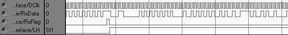
Figure 6 Receive physical layer frame waveform
5. Low power consumption of RTL level and physical design
The low-power implementation of RTL-level physical design has a lot to do with the EDA software selected. Under the 0.35um CMOS process, Synopsys' Design Compiler is used for low-power synthesis, and the layout is based on Cadence's SOC Encounter platform. Using Cadence's Voltage Storm to analyze its gate-level power consumption, the dynamic power consumption is 103.6617mw.
6. Conclusion
Compared with the traditional MSP430 + TRF6903 scheme, the wireless sensor network SOC chip has more advantages. The former has better reliability, power consumption and area. This solution was successfully verified on the FPGA verification platform. The designed operating frequency is 20Mhz, and the speed transmission rate reaches 64kbps, which meets the wireless sensor network transmission speed requirements; and the back-end design of the chip is implemented on Cadence's digital back-end platform. The working frequency can be Reached 100Mhz.
references:
[1] Wu Weiwei, Wang Weidong, Wei Guo. Wireless sensor network based on ultra-wideband technology. ZTE Technology, 2005.4
[2] Dai Hongwei, Guo Wei, Han Zeyao. A low-power SoC chip clock management strategy. Microelectronics and Computing, 2005 Vol.22 No.3
[3] Wang Zuodong, Wei Shaojun. Research and development of low-power design in SOC era. Microelectronics, 2005 Vol.35 No.2
[4] Keshab K. Parhi. VLSI Digital Signal Processing
Systems Design and ImplementaTIon. Machinery Industry Press, 2003
[5] Lu Xiyu, Tang Kun, Cui Huijuan. Low power consumption design based on embedded system. Microcomputer Information, 2005 No. 2
APM variable power supply inherits the functional design and maintains the high power density characteristic.Standard communication interface includes RS232/RS485/USB/LAN,GPIB is optional.Users can choose the switch mode power supply that fits their testing requirements perfectly.
Some features as below:
- With accurate voltage and current measurement capability.
- Coded Knob, multifunctional keyboard.
- Standard RS232/RS485/USB/LAN communication interfaces, GPIB is optional.
- Remote sensing line voltage drop compensation.
- Equips with LIST waveform editing function.
- Use the Standard Commands for Programmable Instrumentation(SCPI) communication protocol.
- Have obtained CE certification.
150V DC Source System,High Current Power Supply,Apm Tech Power Supply,150V Dc Power Source
APM Technologies Ltd , https://www.apmpowersupply.com