LED dot matrix is ​​an important display terminal for public information, and large-screen LED dot matrix display screens can be applied in many occasions. Large-screen display technology is more difficult to display than small and medium-sized screens, because its screen is large, the number of LED points is large, and each point is refreshed in a very short time, which requires that the scanning rate must be very high, in addition, the large screen as information The important media released have high requirements for stability, reliability and scalability. Only well-designed control circuits can meet the above requirements. This article focuses on several design methods for control circuits in LED large-screen design, and gives different solutions for different design requirements.
1LED large screen system works
A typical LED large-screen display system is mainly composed of a signal control system, a scanning and driving circuit, and an LED array. The system structure is shown in FIG. At present, the screen design of most LED displays adopts a modular structure, and its basic unit is an LED display unit module, the screen size and shape can be flexibly changed, and the display installation and maintenance are also very convenient.
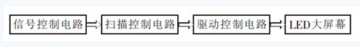
Figure 1 system block diagram
The signal control system is a microcomputer system, a single chip system, a microcomputer Z single-chip master-slave control system, a programmable logic device control system, an infrared remote control system, a paging receiving and control system, and the like. The task of the signal control system is to generate or receive the digital signals required for LED display and to control the various components of the entire LED display system to work in accordance with a certain division of labor and timing. The row driver circuit is mostly a triode array, which supplies a large current to the LED. The column drive consists of a serial-in and parallel shift register and a latch (or a shift register with a latch function).
After the data to be displayed is ready, the control system first sends the first row of data into the shift register and latches, and then the row scan circuit strobes the first row of the LED array, after lighting for a period of time, then displays the subsequent row in the same manner. Until the display content of one frame is completed, this cycle is repeated. According to the principle of persistence of vision, it is possible to achieve 24f/s display so that the naked eye has no obvious pause, which is equivalent to the response time of 40ms or less. When the LED display screen is large in area, the amount of data transmitted is also very large, thereby increasing the response time of the display system to cause flicker, and in order to improve the visual effect, the parallel display can be performed in sections.
In the high-speed dynamic display, the luminance of the LED is proportional to the illumination time in the scanning period, so the gray scale display can be realized by modulating the ratio of the illumination time of the LED to the scan period (ie, the duty ratio).
2LED large screen control circuit design
The design of the control circuit is the core of the large-screen system design. The control circuit design includes the design of the signal control system, the scanning circuit and the driving circuit. The design of the control circuit is generally controlled by data memory, data buffer, counter, synchronous controller, and read/write control. , master-slave controller, address controller, frame memory, data selector, gray modulator, shift register, etc. At present, LED display control circuit design widely uses two types of devices as its control core to achieve, one is the single-chip control system, and the other is the programmable logic device.
2.1. Control circuit design based on single chip microcomputer
There are two main schemes for the control circuit based on single-chip microcomputer. One is a single-chip microcomputer as the main control device to control and coordinate the display of the entire display system of the large screen. One is that the multi-chip microcomputer constitutes a multi-processor, one of which is used as the main CPU, and the other is used as the main CPU. The sub CPUs together control the display of the large screen.
Figure 2 is a schematic diagram of a control circuit mechanism using a single-chip CPU design, using the 89C52 microcontroller as the control core. The MCU receives the display data sent from the PC or other information source and stores it in the Flash. At the same time, the RAM6264 is used as the field display buffer area to realize different display broadcast modes. The 89C52 controls the changeover switches C1, C3 and C2, and C4 alternately reads and writes data to and from the frame memories A and B, and performs parallel 5 serial conversion of the read data to the display screen for display refresh. The automatic address generator is composed of four counters connected in series, and is equipped with an oscillating circuit to provide a counting clock. For a monochrome screen of M×N pixels, when the refresh frequency is 60 Hz, the counting frequency is M×N×60 Hz. Multi-grayscale color large screen, the color of the image should be reproduced before the data is sent to the display screen, and the processing speed of the data is higher. The use of single-chip control may not meet the requirements in terms of speed.
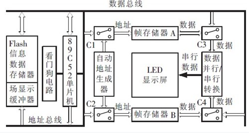
Figure 2 Schematic diagram of the structure of the single-chip CPU control circuit
Since many I/O ports of MCUs have more than 15mA driving capability and are relatively inexpensive, multi-processor solutions are also used in the design of large screens. The basic characteristics of the system are: a display group has multiple processors, including a main CPU and multiple sub-CPUs, and its structure is shown in Figure 3. The task of the main CPU is to obtain display information through data acquisition or communication with the outside world, and then transmit it to the sub-CPU. The main CPU is also responsible for scanning and transmitting display synchronization information. The sub CPU receives the data information of the main CPU and stores it in the internal RAM. Then, according to the control information sent by the main CPU, select the appropriate column output port for column scanning. Assuming that each sub-CPU can be used as an output port with a maximum number of pins of m and the number of columns of each LED matrix is ​​n, the maximum number of LED blocks that can be driven per chip is m/n. One or several pieces of >LED block, flexible and easy to expand, while reducing the burden on the main CPU and increasing the refresh rate of the dot matrix.
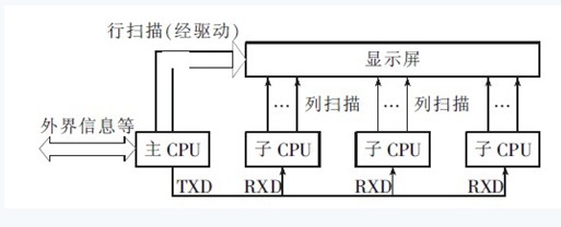
Figure 3 Schematic diagram of multi-CPU control circuit structure
In the large-screen design of multi-screen display, this scheme is ideal. A separate sub-CPU is used for column scanning on different display screens, and then a unified line scan is performed by the main CPU. Although the control circuit uses many components, The circuit structure is simple and easy to implement.
2.2 Control circuit design based on CPLD/FPGA
The frequency of the frequency image signal is high: the data volume is large, real-time processing is required, and the digital logic of the LED large-screen circuit is quite complicated. The CPLD/FPGA design control circuit can simplify the system structure and facilitate debugging. Figure 4 is a schematic diagram of the CPLD/FPGA design control circuit. CPLD/FPGA devices are used to integrate a large number of circuits such as synchronous control, master-slave control, read-write control and gray-scale modulation, which makes image data processing faster, images more stable, and the system is compact and reliable. Increased.
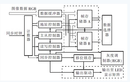
Figure 4CPLD / FPGA control circuit schematic
The functional modules other than the dotted line in Figure 4 have CPLD/FPGA programming implementations, and the complex hardware circuit design is replaced by software programming. Compared with the single-chip control circuit of Figure 2, the circuit structure is obviously more compact, the circuit area is reduced and the reliability is enhanced, and the debugging is also simpler. Because CPLD/FPGA can process multiple processes in parallel, compared with the task of the single-chip microcomputer. The sequential processing is more efficient and the refresh rate of the dot matrix is ​​also increased.
In addition, the on-chip resources of programmable logic devices are becoming more and more abundant. Many devices integrate RAM blocks internally. For example, Altera's cost-effective FPGA Hurricane EP1C6 integrates 20 RAMs internally. Modules, each with a capacity of 4Kbit, can be set to single-port RAM by software. , dual port RAM, FIFO, etc., to meet the needs of the system for data processing. For example, when designing a grayscale modulator, the higher the grayscale level of color reproduction, the higher the processing speed of the data while maintaining the same refresh frequency. At this time, the internal RAM of the FPGA can be used. The block is set to a dual port RAM. As a buffer for gradation modulation, while reading the data in the frame memory, the data read last time is gradated, and the two are alternately performed, thereby speeding up the data processing rate. In the large screen design with high integration and stability requirements of the display system: the gray level of the image is more convenient, it is more convenient to design the control circuit by using the programmable logic device.
Other control circuit design schemes use MCU technology and EDA technology, use MCU to realize data processing, storage and communication functions, CPLD/FPGA realizes data gray-scale modulation, scanning display and other functions. This kind of scheme does not have high resource requirements for single-chip microcomputer and CPLD/FPGA, and the circuit design is relatively easy, which not only ensures the display effect, but also saves the design cost.
The application of 2.3 embedded system in large screen design
Because embedded computer technology has the advantage that single-chip microcomputer can't match: the instruction execution speed is one order of magnitude higher than that of ordinary single-chip microcomputer, and supports large-capacity storage space: wide-range memory interface type, high-bit width data bus, various peripheral communication interfaces, especially The use of the embedded operating system can more effectively manage the allocation of system resources. Through its efficient scheduling algorithm, the design of the entire application can be implemented in a multi-tasking manner, which greatly improves the operating speed and reliability of the system. . The control circuit design of the embedded system based on Linux is shown in Figure 5.
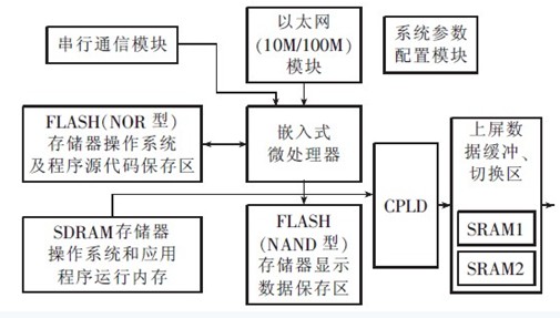
Figure 5 Schematic diagram of embedded system control circuit based on Linux
2. 4 large screen display drive scheme
There are three types of LED large-screen drive solutions: serial control drive mode: parallel control drive mode and application-specific integrated chip driver. The serial control driving method is to send the displayed data to the dot matrix driving circuit through serial mode, which is characterized by simple line connection, convenient debugging, and high reliability of the unit. The chips selectable by the serial control driving method are: MC4094, 74LS595, 9094, etc., the line driver requires a large power, generally driven by a high-power triode, the line scan can be controlled by a three-eight decoder, etc., since the serial-in and out-out chips can be cascaded, the cascade of LED units Support is provided.
The parallel control driving method sends the displayed data to the point driving circuit in parallel, which has the advantage that the data refresh rate is fast. The parallel drive mode can select the latch chip of 74LS374, which is controlled by the end-to-end connection: the drive is formed together. The parallel drive scheme is easy to control and the system input cost is low. Highly integrated dedicated driver chip such as ZQL9701 set: column control and some peripheral drive circuits in one unit, which makes the unit control: the drive is simpler, the stability of the system is more reliable, and the ZQL9701 will make the display gray scale of the system reach 256. Level, but the system cost is higher. For small and medium-sized production and application, the previous two drive solutions should be the main ones. Large-scale production and high-demand applications can be driven by dedicated integrated chip drivers.
3 Conclusion
The design scheme of the LED large-screen control circuit has its own characteristics. In actual engineering applications, different design schemes can be selected according to the needs. When designing large screens with low monochrome and gray scale, the design scheme based on single-chip microcomputer can be adopted, and high design is required. For difficult graphics dynamic multi-effect display and multi-gray level display, you should choose a design based on programmable logic device or a design based on embedded technology.
Stylus Pen Tip,Stylus Pencil Tip,Carbon Fiber Pen Tip,Carbon Fiber Stylus Pen Tip
Shenzhen Ruidian Technology CO., Ltd , https://www.szwisonen.com