In order to communicate with the SPI standard peripheral interface device, the microcontroller (MCU) system must use the SPI (Serial Peripheral Interface) bus. SPI bus system is a synchronous serial peripheral interface proposed by Motorola. It has the characteristics of less signal lines, simple protocol and fast transmission speed. Therefore, many peripheral devices use SPI bus, such as Flash RAM, A/D converter. , LED displays, MCUs, and computer networks. The SPI interface in the MCU can be directly connected to various standard peripheral devices manufactured by various manufacturers through configuration.
For those MCUs that do not have the SPI interface function, the function of the SPI interface is simulated by software controlling the MCU I/O port. However, using software to emulate the functions of the SPI interface, the operating speed is very slow, and the software that requires master-slave devices fits together very well. If the SPI interface function is implemented with a hardware circuit inside the SCM chip, if the hardware is not much increased, the transmission speed can be greatly increased (up to a quarter of the frequency of the main device), reducing the burden on the software. Extremely convenient.
When the SPI interface is working, there is no reply signal, and the data does not need a check bit when it is sent. Therefore, the software of the master-slave device must fully meet the timing requirements of the SPI, otherwise the data transmission is prone to errors. This article through the MCU SPI interface module design, analysis of data transmission of various error conditions, and for various situations, enhance the error handling capabilities of the SPI interface.
1 SPR setting errorWhen the slave clock frequency is less than the master clock frequency, if the SCK rate is set too fast, the received data will be incorrect (it is difficult for the SPI interface to judge whether the received data is correct, but to process it in software).
The speed of the entire system is affected by three factors: the master clock CLK, the slave clock CLK slave, and the synchronous serial clock SCK, where SCK is the frequency division of the CLK master, and the CLK slave and the CLK master are asynchronous. To make SCK detectable from the device without errors, the slave clock CLK must be fast enough. The following takes the 4-octave waveform with SCK as the CLK master as an example to analyze the relationship between the synchronous serial clock, the master clock, and the slave clock.
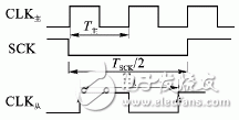
Figure 1 Relationship between master clock and SCK
As shown in Figure 1, when T is
In Fig. 2, when T is from ≥TSCK/2=2T main, the low level of SCK cannot be detected at both rising edges of clk_s, so that the slave device will miss one SCK. Under certain phase conditions, even if CLK can detect the low level of SCK from chance, there is no guarantee that it will continue to detect the next SCK. As long as one SCK is missed, it is equivalent to a bit missing from the serial data, and the data that continues to be received/transmitted afterwards is all wrong.
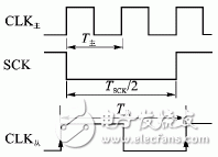
Figure 2 Relationship between master clock and SCK
Based on the above analysis, the relationship between SPR and master-slave clock ratio is listed in Table 1.
Table 1 Relationship between SPR setting and master/slave clock cycle ratio
Before sending data, set SPR according to Table 1. SPR setting errors can be completely avoided.
2 Mode error (MODF)The mode error indicates that the setting of the master-slave mode selection and the connection of the pin SS are inconsistent.
When the device is operating in master mode (MSTR = 1), its chip select signal SS pin must be tied high. During data transmission, if its SS jumps from high to low, at the falling edge of SS, the SPI module will detect a mode error and set the MODF bit to force the device to switch from master mode to slave mode ( Even if MSTR = 0), the internal counter counter is cleared, and the ongoing data transfer ends as shown in Figure 3(a).
For the slave mode (MSTR=0), when there is no data transfer, the SS high level indicates that the slave device is not selected, the slave device does not work, and the MISO output is high impedance; during data transmission, the chip select signal SS must be pulled low Level, and SS is not allowed to jump. If SS jumps from low level to high level, on the SS edge, the SPI module will also detect a mode error, clear the internal counter, and end the ongoing data transfer. It will not resume operation until the SS recovers to a low level and re-enables SPEN=1, as shown in Figure 3(b).
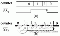
Figure 3 Mode error detection
3 Overflow error (OVR)An overflow error means that the last data overwrites the previous data when multiple data are transmitted continuously.
The status flag SPIF indicates that data transmission is in progress and it has a greater impact on the data transmission. The master's SPIF is asserted by the data register's empty flag, SPTE=0, while the slave's SPIF is valid only due to the first received SCK transition and is also due to the slave SPIF and master. SCK is asynchronous, so the slave device's transfer flag SPIF has a certain lag from the master's transfer flag SPIF. As shown in Fig. 4, when the master device continuously transmits two data, it may cause the transfer flag of the slave device to overlap with the transfer flag of the next data of the master device (dotted lines and shaded portions in FIG. 4). The incoming data must be overwritten, and the second data must be received/send inevitably, resulting in an overflow error.
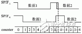
Figure 4 overflow error
Through the analysis of the waveform of the slave device, it is found that the first clock cycle after counter=8, the transmission of the last bit of data has been completed. When the data has been transmitted/received, the length of the counter=8 state has no effect on the correctness of the data, so the state of counter=8 can be shortened to avoid overlapping of the previous SPIF and the subsequent SPIF. In this way, overflow errors at this stage are avoided from the hardware.
However, if the slave device is not operating fast enough or the software is processing something else, if the received data on the SPI interface has not been read yet, and a new data is received, an overflow error will still occur. At this point, the SPI interface protects the previous data from being overwritten, discards the newly received data, sets the overflow flag OVR=1, and sends an interrupt signal (if the interrupt is enabled) to notify the slave device to read the data in time.
4 Offset error (OFST)The SPI interface generally requires the slave device to work first before the master device begins to send data. Sometimes in the process of sending data out of the master device, the slave device starts to work, or the SCK is interfered by the outside world. The slave device fails to receive 8 SCKs accurately. As shown in Figure 5, the eight SCKs received from the device actually belong to the SCK master where the master sends two adjacent data. At this time, the SPIF of the master device and the SPIF of the slave device will overlap, and the data will be misaligned. If the slave device does not correct this, the data reception/transmission will always be wrong.
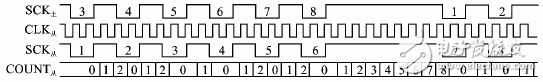
Figure 5 Offset error
In a data transmission process, SPR is not allowed to change, that is, SCK is uniform, and can be seen from Figure 5, the eight SCK received from the device is not uniform, they belong to two data, Therefore, the SCK duty can be calculated to determine whether an offset error has occurred. After analysis, the value of the number n of clock cycles when SCK=1 is normal satisfies the following relationship:
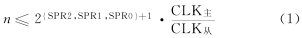
However, since the master-slave clock is asynchronous and has been rounded, the count value COUNT of the clock cycle when SCK=1 is normal should satisfy:

For example, in FIG. 5, the maximum value COUNT(max) of COUNT=2 or 1 can be considered as normal. However, when COUNT(max)=8 appears, it can be determined that an offset error has occurred. In the actual design, the first COUNT(max) value is recorded first. If there is a COUNT(max) that later differs from the recorded value by more than one, it is known that there is an offset error OFST.
occur. The SPI interface sets SPIF=1 in the "non-uniform" place and then prepares for the first SCK of the next data. The number of bits in the COUNT is fixed to 8 bits. To avoid counting from 00H again when overflowing, counting stops when the count reaches ffH.
5 Other errorsImproper settings, or external interference, data transmission will inevitably lead to errors, or sometimes software to determine the type of error is unclear, there must be a way to force the SPI interface to recover from the error state. When SPI does not work, ie when SPEN = 0, clear almost all internal states of the SPI module (except special registers). If the software receives data, it can discover that the data is in error. No matter what the error is, you can forcefully stop the SPI and retransmit the data. For example, in Offset Error (OFST), if SPR2, SPR1, and SPR0 are properly set, SCK can also appear to be “uniformâ€. It is impossible for the SPI interface hardware itself to detect errors. If the user software can find an error, then it is possible to forcibly stop the transmission of the SPI, so as to avoid the error from continuing.
ConclusionThis article analyzes various error conditions in data transmission between SPI interfaces and enhances the ability of the SPI interface to handle errors. For some transmission errors, the SPI interface can detect it by setting the various error status registers and doing the corresponding processing. However, some errors are caused by the hardware itself and cannot be detected. Therefore, in the application, if the correctness of the data is high, besides meeting the timing requirements of the SPI interface in software, it also needs to be properly handled in the software.
SMC Board To Board Connector Section.
Compact high density design
Design of super reliable double beam contact
High speed signal transmission rate up to 3 Gbit / S
Polarization to ensure accurate connection
Locating pin for PCB placement
Welded bracket for secure PCB
Wide operating temperature range
Height range of non matching stack
For full automation board components
SMC Board To Board Connector Section
ShenZhen Antenk Electronics Co,Ltd , https://www.antenkcon.com