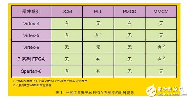
Grasping DCM, PLL, PMCD, and MMCM knowledge is the foundation of a robust and reliable clock design strategy. Xilinx provides a wealth of clock resources in its FPGAs, and most designers will use them more or less in their FPGA designs. But for FPGA design novices, when to use which of the four major types of DCM, PLL, PMCD and MMCM, they are quite confused. None of Xilinx's existing FPGAs contains these four resources (see Table 1).
Each of these four categories is specific to a particular application. For example, the Digital Clock Manager (DCM) is suitable for implementing a delay phase locked loop (DLL), a digital frequency synthesizer, a digital phase shifter, or a digital spectrum spreader. DCM is also ideal for mirroring, transmitting or re-buffering clock signals. Another clock resource phase matching clock divider (PMCD) can be used to implement a phase matching assigned clock or a phase matched delayed clock.
The phase-locked loop (PLL) and mixed-mode clock manager (MMCM) handle many of the same things, such as frequency synthesis, internal and external clock jitter filtering, and clock skew. These two resources can also be used to mirror, send or rebuffer clock signals.
Keeping these general usage in mind when thinking about design implementation details helps to clarify the idea of ​​clock selection. For long-term product development planning, compatibility between individual device families should be considered when developing an appropriate clocking strategy. Let's take a closer look at these clock resources.
You can use DCM to multiply the input clock signal of the clock source to generate a high frequency clock signal. Similarly, the input clock signal from the high frequency clock source can be divided to generate a low frequency clock signal.
Digital clock manager
As the name implies, the Digital Clock Manager (DCM) is a module for managing the clock architecture and facilitating clock signal shaping and manipulation. The DCM includes a delay phase-locked loop (DLL) that removes the skew of the DCM output clock signal based on the input clock signal to avoid clock distribution delay.
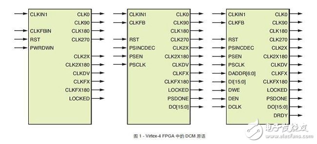
The DLL contains a delay element and a control logic link. The output of the delay element is the input clock delay. The delay time depends on the position of the delay element in the delay link. This delay is reflected in the phase change or phase shift for the original clock, which is called the "digital phase shift". Figure 1 shows a typical DCM module in a Virtex-4 device. According to the Virtex-4 FPGA User Guide (UG070, version 2.6), there are three different DCM primitives in Virtex-4.
In general, DLLs are similar to PLLs. But unlike PLLs, DLLs do not contain a voltage controlled oscillator (VCO). The PLL always stores phase and frequency information, while the DLL only stores phase information. Therefore, the DLL is slightly more stable than the PLL. Both DLL and PLL types can be designed using analog and digital techniques, or a mixture of two technologies. But the DCM in Xilinx devices is fully digital.
Since DCM can introduce delays into the clock path, for example, you can use DCM to accurately generate timing for row and column access strobe signals for DRAM. Similarly, individual data bits on the data bus can arrive at different times. In order to properly sample the data bits, the clock signal at the receiving end must be properly synchronized with the arrival of all data bits. If the receiver uses a transmit clock, it may be required to delay the clock signal from the sender to the receiver.
Sometimes the design may require a higher clock frequency to run the logic on the FPGA. However, only clock sources with low frequency outputs are available. At this point, DCM can be used to multiply the input clock signal of the clock source to generate a high frequency clock signal. Similarly, the input clock signal from the high frequency clock source can be divided to generate a low frequency clock signal. This technique is called "digital frequency synthesis."
Designers use a spread-spectrum clock and modulate the clock signal to reduce the peak electromagnetic radiation of the clock signal. The peak of the unmodulated clock signal produces high electromagnetic radiation. But after modulation, the electromagnetic radiation is spread over a range of clock frequencies, reducing the radiation at all frequencies. In general, if you need to meet certain maximum electromagnetic radiation requirements and perform high-speed processing on the FPGA (such as the deserializer used by the receiver in a communication system), you need to use a spread-spectrum clock. Therefore, the DCM in the FPGA will multiply the input spread spectrum clock signal to generate a high frequency clock signal internally. The output of the DCM must accurately follow the spread spectrum clock to keep the phase and frequency aligned and update the skew and phase shift. Deterioration of DCM phase and frequency alignment can reduce the skew margin of the receiver.
Creating a mirror of the clock requires sending the clock signal out of the FPGA device and then receiving it back. This method can be used to skew the board-level clock signals of multiple devices. The DCM can send clock signals from the FPGA to another device. This is because the FPGA's input clock signal cannot be routed directly to the output pin and no such routing path is available. If only the clock signal needs to be sent, the DCM is used to send the clock signal to the output pin to ensure the fidelity of the signal. Alternatively, you can choose to connect the DCM output to the ODDR trigger before the clock signal is sent. Of course, you can choose not to use DCM, only use ODDR to send the clock signal. Often clock drivers need to drive clock signals to multiple components of the design. This can increase the load on the clock driver, causing clock skew and other problems. In this case, you need to use a clock buffer to balance the load.
The clock can be connected to a series of logic blocks on the FPGA. To ensure that the clock signal has proper rise and fall times on registers remote from the clock source (and thus control the input and output delays within the allowable range), a clock buffer needs to be inserted between the clock driver and the load. The DCM can be used as a clock buffer between the clock input pin and the logic block.
Finally, DCM can also be used to convert the input clock signal to a differential I/O standard signal. For example, the DCM can convert the incoming LVTTL clock signal into an LVDS clock signal for transmission.
Phase matching clock divider
Designers can use a phase-matched clock divider (PMCD) to generate a phase-matched divided-input clock signal. This is similar to the DCM frequency synthesis of the divided clock. The PMCD can also generate a clock signal with phase matching but delay in the design. In the latter case, the PCMD is capable of maintaining edge alignment, phase relationship, and skew between the input clock signal and other PMCD input clock signals. Unlike DCM, the clock signal generated by the existing PMCD in Xilinx devices is divided by 2, 4, and 8 only when the value of the divider is configurable. This means that the frequency of the clock signal generated by the PMCD is 1/2, 1/4 and 1/8 of the input clock signal. In Xilinx devices such as the Virtex-4 FPGA, the PMCD is in close proximity to the DCM and is in the same column. There are two PMCD-DCM pairs in each column. Therefore the output of the DCM can drive the input of the PMCD.
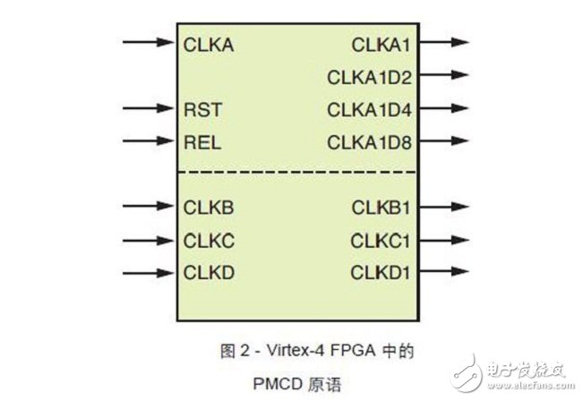
Since DCM is also responsible for handling skew, designers can use PMCD without DCM as long as there is no need to skew the clock. It is also possible to connect two PMCDs in a column through dedicated pins. Figure 2 shows the PMCD primitives in a Virtex-4 device. See the Virtex-4 FPGA User Guide (UG070, version 2.6) for details.
Shareconn development Co.,Ltd manufacture series flexible flat cables, we can produce pitch 0.5mm,1.0mm,1.27mm, 2.54mm flat cables.
Our factory is qualified with ISO9001:2008, ISO13485:2003 and TS16949:2009 certificates, equipped with high-end automatic production equipment, like automatic crimping machines, automatic wire cutting and crimping machines, automatic crimping and tinned plate machines, etc. Meanwhile, we have our own laboratory to support the testing requirements from our suppliers and 100% checking before shipment. To assure the product and the comprehensive competence, we introduce high-level technical talents and management personnel as well as well-trained staff, and improve ourselves in many ways, like the quality, price, delivery, service, etc. Now, Shareconn has been the best supplier and partner for many customers.
Flexible Flat Cable,Flexible Flat Cable With Connector,Pvc Flexible Flat Cable,Electric Wire Flexible Flat Cable
Shareconn Development CO.,LTD , http://www.share-conn.com