It is well known that synchronous rectifiers can replace the rectifier junction voltage with a lower resistive switching voltage drop, greatly improving power efficiency. The challenge is to develop robust control strategies that drive components and maximize their benefits. Synchronous rectifiers are more challenging to operate in non-continuous flyback than continuous flyback. Figure 1 is a simplified schematic diagram of a flyback synchronous rectifier and associated waveforms. At t=0, the main switch Q1 is turned on, and its drain current rapidly increases.
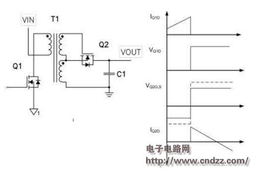
Figure 1: Self-driven synchronous rectifiers cannot naturally rectify in discontinuous flyback)
The switch is then turned off and the voltage at the end of the transformer winding line rises until the body diode of Q2 clamps the voltage across the transformer below the output voltage. Note that the gate of Q2 is more active than its source. In this way, the current can be rectified not only from the body diode to the MOSFET channel, but also improves the rectification efficiency. The circuit is effectively latched by the forward gate-to-source voltage connected by the transformer.
During this time, the magnetizing inductance will discharge and turn in the opposite direction. To exit this state, Q1 must be turned on to reverse the Q2 gate voltage to turn it off. This is a very stressful event. Both transistors are turned on at the same time, and the current and voltage peaks are very high. This simple circuit is typically operated in a continuously conducting state with at least one switch in the conducting state throughout the process.
The key to making synchronous rectifiers work in non-continuous flybacks is to have them work like the diodes they replace, that is, they must be turned off when the current is diverted. The traditional approach is to use a snubber current transformer that provides a positive drive voltage when the current is in the correct direction and reverses the drive when the current is in the opposite direction. The short board is the cost and size of the current transformer and several discrete components for buffering.
Several companies, such as Texas Instruments, have developed ICs that replace the current-sensing driver circuits shown in Figure 2. The synchronous rectifier is moved to the low side of the transformer and the timing and gate drive functions are provided by the control chip. The advantage is that the source is directly connected to the ground and the gate can be driven directly. 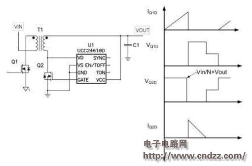
Figure 2: The IC properly drives the gate of the synchronous rectifier by sensing the voltage steering of the entire drain voltage.
Since the device operates by monitoring the drain-to-source voltage, the circuit is not prone to noise when the source connects the system to the ground. This circuit now plays a non-continuous flyback, and the right side shows some ideal waveforms. Of particular concern is the voltage stress on the output rectifier, which is the drain voltage (VD) connection on the IC. This voltage will actually be higher due to ringing. Ideally, however, the voltage is equal to the reflected input voltage plus the output voltage. If the output voltage is greater than 5V, or if a wide input voltage is supported, the voltage at that node will easily exceed the IC50V's rated voltage.
Figure 3 is a simple, low-cost circuit with an operating voltage rating roughly equivalent to a VD pin that includes two components. As shown on the right side of the figure, the voltage on the VD pin is limited by the output voltage. When primary FET Q1 is turned on, the voltage across the drains of Q2 and Q3 is equal to the reflected input voltage plus the output voltage. Since the gate of Q3 is connected to the output voltage, the source voltage is approximately lower than the threshold voltage. When Q2 is turned on, the Q3 body diode turns on and its source is dropped below the output voltage, which enhances Q3 performance and connects the VD pin to the Q3 drain. 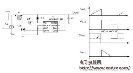
Figure 3: A simple clamp can extend the available operating voltage range. )
In summary, users cannot create self-driven synchronous rectifiers for non-continuous flyback converters. We need to add some circuits to judge the time to drive them, and drive current transformers and semiconductor circuits can achieve this application, where semiconductor circuits have a comparative advantage in size and cost. Several circuits have been developed by several vendors, but they may require an appropriate interface for buffering to match the high voltages and currents in the power supply.
Light-resistant design ,and support single and muilt touch points,widely use to financial telecom service,Adverstisement show,Industrial control ,public query ,self-service,E-education ,and games etc aera.Ultra-thin, ultra-narrow design, no matter whether it is external or built-in, it can adapt to various needs without affecting the appearance and saving built-in space. Infrared sensing principle, simple finishing, LED die, stable performance, high touch precision and long life.The unique installation method makes the installation of the client a breeze.The surface of the aluminum alloy is sprayed and oxidized, and the whole is delicate, simple, generous and multi-touch. Simple operation, USB connection, plug and play.
Picture show:


Diy Infrared Touch Frame,Infrared Touch Screen Kit,Install Infrared Touch Frame,Ir Touch Frame Diy,Usb Infrared Touch Screen,Outdoor Infrared Touch Screen
ShenZhen GreenTouch Technology Co.,Ltd , https://www.bbstouch.com