0 Preface
Switched Reluctance Motor Drive System (SRD) is a new type of stepless speed regulation system developed by the combination of power electronics technology, control technology and computer technology with traditional reluctance motors. Power converter is an important part of the switched reluctance motor drive system, which accounts for a large proportion of the motor cost. Its performance will directly affect the working efficiency and reliability of the motor. The difference in the topology of the power converter is mainly reflected in the difference in the way the motor windings feed back energy. This paper will take the switching reluctance motor power converter as the research object.
1 Switched reluctance motor power conversion circuit
1.1 Introduction to Power Converter
The power converter regulates different loads to operate at rated power, and also has the effect of being unaffected by grid fluctuations. Power converters are implemented by power electronics, both DC power converters and AC power converters. The principle is to adjust the on-time in one cycle or to adjust several continuous on or off times in several cycles to change the motor output power.
Power electronic devices are widely used in speed control systems and various power conversion circuits. Power electronic devices operating in switching mode are the basis and core of switching reluctance motor power conversion circuits. At present, the most commonly used power switching devices are as follows: thyristor (SCR), bipolar power transistor (GTR), turn-off thyristor (GTO), power field effect transistor (Power MOSFET), insulated gate bipolar Transistor (IGBT). In this paper, the power conversion circuit of the switched reluctance motor is selected as the main switching device of IGBT.
1.2 Power converter topology
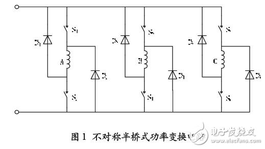
The power converter is an important part of the switched reluctance motor drive system. Its topology has many forms, the difference is mainly in the way that the recovery winding releases the magnetic field energy. Figure 1 shows an asymmetric half-bridge power conversion circuit.
2 power converter design
2.1 Structural characteristics of the new power conversion circuit
The topology of the main circuit of the new power converter is shown in Figure 2. In addition to the dotted boxes I and II in the figure, it is a typical asymmetric half-bridge power conversion circuit. Among them, A, B, C are three-phase windings of SRM; S1 ~ S6 are phase switches; D1 ~ D6 are freewheeling diodes of each phase winding; and the soft-switching auxiliary circuit within the dotted line frame I is composed of resonant inductor Lr, resonant capacitor Cr The auxiliary switch Sch, Sdis and diodes Dch, Dfr are composed; the dotted line frame II is the RCD buffer absorption circuit, which is connected in parallel with the main switch.
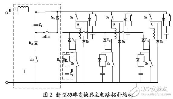
Compared with the traditional half-bridge power conversion circuit, the circuit has the following characteristics: a soft switch auxiliary circuit is added to the circuit, and the soft opening and soft closing of the main switch can be realized as long as the auxiliary switch Sch, Sdis is turned on and off at the appropriate time. The RCD snubber circuit connected in parallel with the main switch can suppress the overvoltage at the time of IGBT turn-off due to the sudden change of the capacitor voltage, and at the same time, can alleviate the fluctuation of the winding flux linkage during the turn-on.
2.2 Analysis of the working principle of the new power conversion circuit
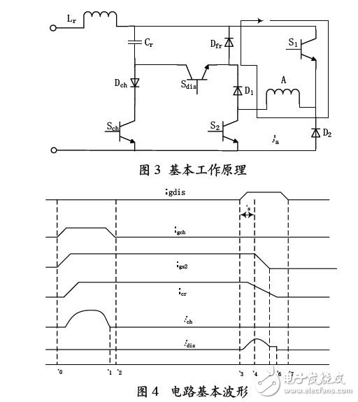
Taking the A-phase winding as an example, the basic operation diagram of the improved circuit is shown in Figure 3. Figure 4 shows the basic waveform of the circuit. One of the switching cycles of the main switch S2 is divided into three phases: charging, PWM modulation and discharging:
(1) During charging (t0 ~ t2 as shown in Figure 4): Before t0, the capacitor Cr has been discharged to zero in the previous cycle. At time t0, Dch is turned on under zero current switching conditions, Cr is charged through inductor Lr, and ends at 1/2 resonant period to t1. Due to the unidirectional conductivity of Dch, ich=0 after time t1, and Sch is turned off at zero current condition at time t2. When t0 is turned on, the DC link voltage drops to zero, and S2 turns on at zero voltage.
(2) During PWM (t2 to t3 as shown in Figure 4): The energy output to the SRM can be controlled by adjusting the duty cycle of the PWM.
(3) During discharge (t3 ~ t7 as shown in Figure 4): At time t3, Sdis turns on, capacitor Cr discharges through Lr, and the discharge path is Cr → Lr → U → S2 → D1 → Sdis.t5 The load current begins to flow through Cr, and Cr is continuously discharged to zero. Finally, at time t6, Vcr=0, diode Dfr turns on, idis=0, load current passes through D1, Dfr and S1.t6, Sdis turns off, idis=0.
ZOOKE provides you with safe and reliable connector products, with 1.0 spacing products providing more possibilities for limited space and creating more value for the research and development and production of terminal products.
1.00 wire to board connectors,1.0 connectors,ZOOKE connectors
Zooke Connectors Co., Ltd. , https://www.zooke.com