
I've always been drawn to electronics, and in today's world of smart technology, field-programmable gate arrays (FPGAs) stand out as truly remarkable tools. If you're aiming to build a career in this fast-evolving field, ignoring FPGAs means falling behind. The future belongs to those who understand and master these powerful devices.
When it comes to high-speed system PCB design for SERDES applications, there are several key considerations to keep in mind:
(1) Microstrip vs. Stripline Routing
Microstrip lines are found on the outer signal layers, separated from a reference plane (GND or VCC) by a dielectric material. This configuration helps minimize signal delay. In contrast, stripline routing is used for inner signal layers between two reference planes, offering better capacitive coupling, easier impedance control, and cleaner signal integrity.
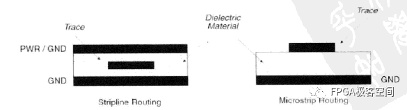
Optimal microstrip and stripline routing can significantly improve signal performance in high-speed designs.
(2) High-Speed Differential Pair Routing
Differential signaling is crucial for high-speed communication. Common methods include edge-coupled microstrip, edge-coupled stripline (ideal for high-speed SERDES), and broadside-coupled microstrip. Each method has its own advantages depending on the application and layout constraints.
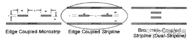
Proper differential pair routing ensures minimal crosstalk and maximum signal integrity.
(3) Bypass Capacitor Placement
Bypass capacitors are essential for filtering high-frequency noise. In FPGA systems, different capacitor values are used based on the speed of the system:
- High-speed systems (100MHz–1GHz): Use 0.01nF to 10nF capacitors within 1cm of Vcc.
- Medium-speed systems (10MHz–100MHz): Use 47nF to 100nF tantalum capacitors within 3cm of Vcc.
- Low-speed systems (<1MHz): Use 470nF to 3300nF capacitors with more flexible placement.
(4) Optimal Capacitor Wiring
To ensure optimal performance, follow these guidelines when wiring bypass capacitors:
- Use large vias to connect capacitor pads and reduce coupling capacitance.
- Use short, wide traces between vias and capacitor pins, or directly connect them.
- Choose capacitors with low ESR (Equivalent Series Resistance).
- Ensure all GND pins or vias are connected to the ground plane.
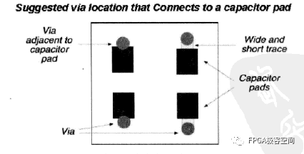
Proper capacitor routing reduces noise and improves power integrity.
(5) Clock Signal Routing
For high-speed clock signals, avoid sawtooth patterns and use straight routing where possible. Route clocks on a single layer if possible, and minimize via usage to prevent reflections and impedance mismatches. Use microstrips on the top layer to reduce delay, and place the ground plane close to the clock layer to reduce noise and crosstalk. If using internal layers, sandwich the clock layer between two ground planes for better isolation.
(6) Coupling and Signal Integrity
Ensure proper impedance matching for differential signals and maintain line widths that accommodate 20% of the signal rise/fall time. Choose connectors rated for the highest frequency in your design. Prefer edge-coupled differential pairs over broadside-coupled ones, and follow the 3S rule to avoid over-coupling and crosstalk.
(7) Noise Filtering
Reduce low-frequency power supply noise by adding shielding or filters at each power entry point. Use 100μF electrolytic capacitors at power input locations. Place decoupling capacitors close to Vcc and GND to suppress high-frequency noise. Keep Vcc and GND planes parallel, separated by a dielectric like FR-4, and add bypass capacitors on other layers for better stability.
(8) Ground Bounce Mitigation
Add decoupling capacitors to each Vcc/GND pair to stabilize the power supply. Use external buffers for high-speed outputs like counters to reduce drive strength. Set unused I/Os to a low output state to act as a virtual ground. Enable slow slew mode for less demanding signals. Control load capacitance and avoid constant clock toggling. Distribute frequently flipped signals evenly across the chip. Route these signals near GND pins to minimize noise. When designing synchronous circuits, try to eliminate transient outputs. Keep power and ground planes apart to neutralize inductance and reduce bounce.
Shenzhen Kaixuanye Technology Co., Ltd. , https://www.icoilne.com