Overview:
Various portable electronic products, such as cameras, video cameras, mobile phones, notebook computers, multimedia players, etc., require power management chips such as DC-DC converters. These portable devices are typically powered by batteries and have a limited total energy. Therefore, the power chip needs to minimize the operating voltage and extend the life of the battery. The operating voltage of the traditional DC-DC is generally above 1.0V. This paper designs a low-voltage starting circuit for a DC-DC step-up switching power supply. The starting voltage is reduced to 0.8V. The circuit uses two different power supply voltage ranges. The oscillator circuit with stable operating frequency uses a voltage detection module to perform reasonable switching, which solves the problem that the circuit cannot work normally under low input voltage, and is in the 0.5μm CMOS process library (VthN=0.72V, VthP=-0.97V). simulation. The simulation results show that VDD can be raised to 3.3V through this step-up switching power supply at a low input voltage of 0.8V.
Overall schematic of the circuit
The DC-DC step-up switching power supply operates at a low input voltage, and the control circuit turns on and off the power tube. When the power tube is turned on, the inductor stores energy; when the power tube is turned off, the inductor releases energy, and the output is output. The capacitor is charged and the output voltage is raised. When the input power is as low as 1.0V or less, if the driving voltage of the DC-DC chip is taken from the input power, the internal circuit of the chip cannot work normally, and the DC-DC cannot be started; if the driving voltage of the DC-DC chip is taken from the output voltage, Again, the chip simply cannot start and perform any boosting actions. In this paper, for the input power supply voltage variation range, in the case of considering the commercial cost, two oscillator circuits are designed: the main oscillator and the auxiliary oscillator. The auxiliary oscillator is powered by the input voltage, and can be started at 0.8V. Before the VDD rises to 1.9V, the power transistor is turned on and off, so that VDD is gradually raised. The main oscillator is powered by the output voltage, VDD. It operates at a more stable frequency after VDD rises to 1.9V, raising and maintaining the output voltage. The overall schematic of the circuit is shown in Figure 1. The circuit includes a main oscillator, a secondary oscillator and their switching circuits, a bandgap reference circuit, a PWM comparator, an overvoltage protection circuit, an overcurrent protection circuit, and the like. 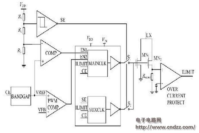
Figure 1 is a schematic diagram of the DC-DC step-up switching power supply chip
(Please read the PDF for details)
Residential Elevators,Indoor Home Elevator,Capsule Lifts For Home,Small Elevators For Homes
XI'AN TYPICAL ELEVATOR CO., LTD , https://www.chinaxiantypical.com