After the diode is turned on, its forward resistance changes slightly with the magnitude of the current. The larger the forward current, the smaller the forward resistance; otherwise, the larger. Using the characteristics between the diode forward current and the forward resistance, some automatic control circuits can be constructed. As shown in Figure 3.1, an automatic control circuit consisting of a diode, also known as an ALC circuit (automatic level control circuit), is often used in recording circuits in magnetic recording devices such as decks.
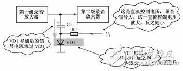
Figure 3.1 Automatic control circuit composed of diodes
3.1 Circuit Analysis Preparation Knowledge Description
The unidirectional conduction characteristics of the diode only indicate that the forward resistance is small and the reverse resistance is large. It does not indicate what specific characteristics are available after the diode is turned on.
After the diode is forwarded, its forward resistance is also related to the amount of forward current flowing through the diode. Although the forward resistance of the diode after forward conduction is relatively small (relative to the reverse resistance), if the forward current is increased, the forward resistance after the diode is turned on will further decrease, that is, the larger the forward current, the positive The smaller the resistance, the greater the opposite.
Unfamiliar circuit function is very unfavorable to the working principle of the circuit. Under the background of understanding the function of the circuit, it can analyze the working principle of the circuit or the function of a certain component in the circuit.
In the recording card of the recorder and the deck, the ALC circuit should control the magnitude of the recording signal during recording. The following specific control requirements are helpful to analyze the diode VD1 automatic control circuit.
(1) When the amplitude of the recorded signal is small, the amplitude of the recorded signal is not controlled.
(2) When the amplitude of the recording signal is large to a certain extent, the amplitude of the recording signal is controlled, that is, the amplitude of the signal is attenuated, and the circuit for controlling the amplitude of the recording signal is the ALC circuit.
(3) After the ALC circuit enters the control state, the larger the recording signal is required, the larger the attenuation of the signal is.
According to the above description, circuit analysis requires that you have a more comprehensive knowledge, which requires accumulation in continuous learning.
3.2. Analysis of the working principle of the circuit The analysis of the working principle of this circuit mainly explains the following points:
(1) If there is no VD1 branch, the recording signals output from the first stage recording amplifier are all added to the second stage recording amplifier. However, with the VD1 branch, the recording signal output from the first-stage recording amplifier may flow through C1 and the turned-on VD1 to the ground to form a shunt attenuation of the recorded signal.
(2) The second key of the circuit analysis is the specific case of the VD1 branch to the ground shunt attenuation of the output signal of the first stage recording amplifier. Obviously, the capacitor C1 in the branch is a capacitor with a large capacity (the polarity is indicated in the C1 circuit symbol, indicating that C1 is an electrolytic capacitor, and the capacity of the electrolytic capacitor is large), so C1 has a path to the recording signal, indicating that this VD1 in a road is a key component for shunting the recorded signal.
(3) It is necessary to understand from the analysis of the shunt branch circuit that if the signal output from the first stage recording amplifier is much more shunted from the VD1 branch, the recording signal flowing into the second stage recording amplifier is small, and vice versa.
(4) There are two cases of VD1 being turned on and off. When VD1 is off, there is no shunting effect on the recording signal, and when it is on, the recording signal is shunted.
(5) A resistor R1 is connected to the positive terminal of VD1, which gives VD1 a control voltage. Obviously this voltage controls VD1 to be turned on or off. Therefore, the voltage sent by R1 is the key to analyzing the turn-on and turn-off of VD1. The biggest difficulty in analyzing this circuit is that after VD1 is turned on, the circuit is analyzed by the relationship between the forward resistance and the on-current after the diode is turned on, that is, the larger the forward current of the diode, the more the forward resistance is. Small, the greater the current flowing through VD1, the smaller the resistance between the positive and negative electrodes, and vice versa.
3.3 General analysis method description of control circuit
The analysis of the control circuit is usually divided into a variety of situations, such as the division of the control signal into large, medium and small. For this circuit, the control of the diode VD1 by the control voltage Ui is divided into the following cases.
(1) When there is no recording signal in the circuit, the DC control voltage Ui is 0, the diode VD1 is turned off, and the smaller the VD1 resistance is, the larger the current flowing through the VD1 is, the smaller the resistance between the positive electrode and the negative electrode is, and vice versa.
3.3 General analysis method description of control circuit
The analysis of the control circuit is usually divided into a variety of situations, such as the division of the control signal into large, medium and small. For this circuit, the control of the diode VD1 by the control voltage Ui is divided into the following cases.
(1) When there is no recording signal in the circuit, the DC control voltage Ui is 0, the diode VD1 is cut off, VD1 and circuit fault analysis. The best way to detect the diode fault in this circuit is to perform an alternative check because the diode is not good. It also affects the control effect of the circuit.
When the diode VD1 is open, there is no control. At this time, the sound will appear when the large signal is recorded, and the small undulating distortion will be small for a while. When the recording signal is very small, the recording can be normal.
When the diode VD1 breaks down, there is no control. At this time, the recording sound is small because the recording signal is shattered by the diode VD1 to the ground.
4 diode limiting circuit and fault handling
The most basic operating state of the diode is both on and off, and this feature can be used to form a limiting circuit. The so-called limiter circuit is to limit the signal amplitude of a certain point in the circuit. When the signal amplitude is large to a certain extent, the amplitude of the signal is not increased. When the amplitude of the signal does not reach the limit, the limiter circuit does not work. A circuit having such a function is called a limiter circuit, and a circuit that uses a diode to perform this function is called a diode limiter circuit. Figure 4.1 shows the diode limiter circuit. In the circuit, A1 is an integrated circuit (a common component),
VT1 and VT2 are triodes (a common component), R1 and R2 are resistors, VD1~
VD6 is a diode.
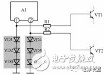
Figure 4.1 Diode Limiting Circuit
4.1 Circuit Analysis Ideas
The idea of ​​analyzing the effects of VD1 and VD2 in the circuit mainly explains the following points:
(1) It can be seen from the circuit that the circuit structures of the two sets of diodes VD1, VD2, VD3 and VD4, VD5, and VD6 are the same. The two sets of diodes play the same role in this circuit, so only analyze the A set of diode circuits can work.
(2) The 1 pin of the integrated circuit A1 is connected to the base of the transistor VT1 through the resistor R1. Obviously, R1 is the signal transmission resistor, and the output signal of the pin 1 is applied to the base of the VT1 through R1, due to the 1 pin and the triode in the integrated circuit A1. There is no DC blocking capacitor between the bases of VT1. According to this circuit structure, it can be judged that the 1 pin of the integrated circuit A1 is an output signal pin, and outputs a composite signal of DC and AC. It is determined that the pin 1 of the integrated circuit A1 is a signal output pin for the purpose of determining the specific role of the diode VD1 in the circuit.
(3) The DC voltage of the output of the 1 pin of the integrated circuit is obviously not very high, and is not high enough for the external diode to be in the on state. The reason is: if the DC voltage output from the 1 pin of the integrated circuit A1 is sufficiently high, then VD1, VD2 It is connected to VD3, and its internal resistance is small. This will shunt the AC signal output from pin 1 of integrated circuit A1 to ground, which will attenuate the signal. Obviously, there is no need to signal the signal in this circuit.
This kind of attenuation, so the conclusion from this angle analysis is that the DC voltage of the output of pin 1 of integrated circuit A1 is not high enough to make VD1, VD2 and VD3 turn on.
(4) From the output of pin 1 of the integrated circuit A1, the DC and AC superimposed signals are passed through the resistor R1 and the base of the triode VT1, and the VT1 is an NPN type triode. If the amplitude of the positive half cycle of the positive half cycle applied to the base of the VT1 is large, The phenomenon causes the base voltage of VT1 to be large and there is a danger of burning out VT1. When the negative half-cycle signal amplitude of the AC signal applied to the base of VT1 is large, there is no burn-out effect on VT1 because the negative polarity signal on the base of VT1 reduces the VT1 base current.
(5) Through the above circuit analysis ideas, it can be preliminarily judged that VD1, VD2, and VD3 in the circuit are limiting protection diode circuits, which prevent the AC signal output from the 1st pin of the integrated circuit A1 from being too large in the positive half cycle and burning out VT1. From the above ideas, further analyze the VD1, VD2, VD3 diode circuits, and if the analysis is logical, it can be explained that the above circuit analysis ideas are correct.
4.2 Diode Limiting Circuit
There are methods for analyzing the operation of various limiter circuits. The amplitude of the signal is divided into two cases:
(1) The operating state of the circuit with a small signal amplitude, that is, the signal amplitude is not so large that the limiting circuit operates, and the limiting circuit does not work.
(2) The working state of the circuit when the signal amplitude is relatively large, that is, the signal amplitude is large enough to allow the amplitude circuit to operate. At this time, the limiting circuit works to limit the signal amplitude.
It is sometimes useful to analyze the working principle of the circuit by drawing the signal waveform. It is especially effective for analyzing the limiting circuit. Figure 4.2 shows the waveform of the signal on the 1 pin of the integrated circuit A1 in the circuit.
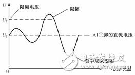
Figure 4.2 Schematic diagram of the signal waveform on pin 1 of integrated circuit A1
In the figure, U1 is the DC voltage in the 1-pin output signal of the integrated circuit A1, and the AC voltage in the 1-pin output signal is "riding" on this DC voltage. U2 is the limit voltage value. Combine the above signal waveform to analyze this diode limiting circuit, when the output of integrated circuit A1 is 1 pin
When the AC voltage in the signal is relatively small, the positive half cycle of the AC signal plus the DC output voltage U1 does not reach the level at which VD1, VD2, and VD3 are turned on. Therefore, all the diodes are turned off, and there is no influence on the AC signal output from the 1 pin. It is added to VT1 through R1.
Assume that the amplitude of the positive half-cycle of the AC signal outputted by pin 1 of the integrated circuit A1 is large during a certain period. See the signal waveform in Figure 8-12. Since the positive half-cycle amplitude of the AC signal plus the DC voltage has exceeded the diodes VD1 and VD2. The voltage value that is forwarded to VD3. If the turn-on voltage of each diode is 0.7V, the turn-on voltage of the three diodes is 2.1V. Since the tube voltage drop after the three diodes are turned on is basically the same, that is, the maximum length of the integrated circuit A1 is 2.1V, the excess half of the AC signal is removed (restricted), and the excess signal is actually reduced to the integrated circuit. The resistance in the circuit of the 1 pin of A1 (not shown). When the amplitude of the 1-pin DC and AC output signals of the integrated circuit A1 is less than 2.1V, this voltage is again
It is impossible to turn on the three diodes, so that the three diodes are again turned from the conduction state to the off state, and there is no limiting effect on the signal.
The manufacturing standard of the European standard plug (two rounds) is carried out according to the CE standard. European standard plugs are used in most European countries such as Germany, Austria, Holland, Sweden, Norway, Finland, and Russia. Since this standard is widely used throughout Europe, we call it the "Continental European" standard. The plug is two cylinders with a span of 19mm. The grounding level is completed by grounding the plugs on both sides. Central and Eastern Europe 7/7 European plugs have embedded pins, similar to French and Belgian sockets. The electrical parameter of the European standard socket is 10A-16A 230ACV AC power supply. The European standard socket is the safe socket in the world. The special grounding is mainly for the safety of people. Therefore, it is also the most widely used plug standard in the world. Note: The Italian standard plug has three cylinders and one wire, and the Danish and Swiss standard plugs have three cylinders into a triangle shape, and both have direct grounding pins.
Uk Plug Adapter,Europe Plug Type,Europe Electric Plug,Plug Converter Eu To Uk
Guangdong Kaihua Electric Appliance Co., Ltd. , https://www.kaihuacable.com