The μPD70320 is a 16-bit single-chip microcontroller from NEC Corporation, part of the V25 series. It offers strong functionality, high reliability, fast performance, and excellent compatibility. The chip integrates 512 bytes of RAM, three I/O ports, eight analog inputs, two DMAs, two timers, two full-duplex asynchronous communication ports, and an interrupt controller alongside its CPU. This makes it ideal for real-time multitasking applications due to its advanced and fast interrupt handling.
The μPD70320 uses a strict CMOS manufacturing process, ensuring stability across a wide voltage range of 3–8V. It supports crystal frequencies from 1–6MHz and is resistant to interference, making it suitable for harsh environments. Its unique dual-bus architecture, combined with 32-bit internal registers and a 6-byte instruction queue, allows it to operate up to 2–4 times faster than the 8088 at the same clock frequency.
Its instruction set is a superset of the 8088, meaning that PC programs can be easily adapted for use on the μPD70320 without the need for special development tools or debugging software, which significantly reduces development costs and speeds up the process.
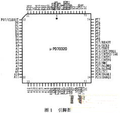
The pin diagram of the μPD70320 is shown in Figure 1.
The μPD70320 shares the same registers and instructions as the 8088 but includes many integrated peripheral components. New features are implemented through special function registers (SFRs), on-chip data areas (IDAs), and special instructions. These SFRs and IDAs are located within the 512-byte on-chip RAM and can be relocated anywhere in the 1MB memory space by setting the value of the on-chip data area address register (IDB) in the SFR. This allows the SFRs to be accessed like regular memory locations.
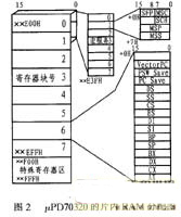
Figure 2 shows the distribution of SFR and IDA. The SFRs are used to control on-chip peripheral units, while the IDAs are mainly used for fast register block switching (RBS) and macro service functions (MSF).
**2. Special Function Register (SFR)**
The μPD70320 has various special function registers, each serving different purposes. Below are some key features:
**2.1 Three I/O Ports**
Each port can be configured as input or output by setting the corresponding bit in the port mode register (PM). Setting a bit to 1 enables input, while setting it to 0 enables output. The port mode control register (PMC) determines whether the port is in control mode or I/O mode. The interface register (P) is used to read or write data to the I/O ports.
**2.2 Eight Analog Comparator Inputs**
Each analog input (PTO–PT7) compares the voltage at the PT terminal with a reference voltage (Vth) divided by a programmable ratio. If the voltage at PT is higher than the reference, the corresponding bit in the PT register is set to 1. The division ratio can be adjusted using the interface mode register (PMT), with values ranging from 01H to 10H. The division value is calculated as Vth × (division ratio)/16. The addresses for PT and PMT are ××F38H and ××F3BH, respectively.
**2.3 Two 16-Bit Timers**
Each timer includes a 16-bit modulus register (MD), a 16-bit decrement register (TD), a control register (TC), a macro service register (TMS), and an interrupt controller (TIC). Timer 0 supports both continuous and single modes, while Timer 1 only operates in continuous mode.
In continuous mode: MD sets the initial value, Bit 5 of TC is set to 1, and the timer starts. When TD reaches 0, MD automatically reloads TD, and the cycle repeats until Bit 5 of TC is cleared.
In single mode: TD0 and MD0 can be used as separate 1-bit registers. When either reaches 0, the timer stops.
**2.4 Two Serial Communication Ports**
Each serial port includes a receive buffer (RB), transmit buffer (TB), mode register (SM), control register (SC), baud rate generator (BRG), communication error register (SE), and several macro service and interrupt registers. Each port has RXD, TXD, and CTS lines. Communication starts when CTS = 0, and reception begins on the falling edge of the start bit. The data frame format includes a start bit, 7 or 8 data bits, a parity bit, and 1 or 2 stop bits, determined by SM settings.
If a communication error occurs, an interrupt is generated, with lower priority than other interrupts. In addition to error interrupts, there are vector interrupts for received data and transmission, along with RBS and MSF support. When an error happens, the corresponding bit in SE is set to 1, where Bit 0 indicates overflow, Bit 1 indicates frame format error, and Bit 2 indicates parity error.
**2.5 Two DMA Controllers**
DMA allows quick data transfer between memory and peripherals. It supports four modes: memory-to-memory I/O (MtoM), memory and I/O (M & I/O), single-step mode (SSM), and burst mode (BM) for MtoM; one transfer mode (STM) and request release mode (DRM) for M & I/O.
- **SSM**: Transfers data byte-by-byte until the specified number of bytes is completed.
- **BM**: Continues transferring until the specified number of bytes is completed.
- **STM**: Performs a single DMA transfer upon request.
- **DRM**: Continues transferring as long as the DMARQ line remains high.
This flexible DMA system enhances system efficiency and reduces CPU load.
Photovoltaic Single-Axis Tracking Bracket
Photovoltaic Single-Axis Tracking Bracket,One Axis Solar Tracker Solar,Solar Tracker Solar Racking Tracker,Solar Racking Tracker System Single-Axis
Hebei Shuobiao New Energy Technology Co., Ltd. , https://www.pvbracketsystem.com