Since the world's first GaN-based blue LED was introduced in 1993, the development of LED manufacturing technology has been remarkable. Currently, commercially available GaN-based LEDs are all fabricated on sapphire substrates or SiC substrates. However, due to high hardness, poor conductivity and thermal conductivity, sapphire brings a lot of inconvenience to the processing and application of later devices. SiC also has the disadvantages of high hardness and high cost, and the Si substrate with relatively cheap price has excellent The advantages of thermal conductivity and mature device processing technology, so Si substrate GaN-based LED manufacturing technology has received widespread attention in the industry.
At present, Japan Nichia Corporation monopolizes the patented technology of GaN-based LEDs on sapphire substrates. CREE Corporation of the United States monopolizes the patented technology of GaN-based LEDs on SiC substrates. Therefore, the development of GaN-based LED production technology on other substrates has become a hot spot in the world. Nanchang University cooperated with Xiamen Hualian Electronics Co., Ltd. to undertake the National 863 Program “Power-based GaN-based LED manufacturing technology based on Si substrateâ€. After nearly three years of research and development, it has passed the acceptance of the Ministry of Science and Technology.
1 Si substrate LED chip manufacturing
1.1 Technical route
GaN is grown on a Si substrate to produce an LED blue chip.
Process flow: growing AlN buffer layer on Si substrate→ growing n-type GaN→ growing InGaN/GaN multi-quantum well light-emitting layer→ growing p-type AIGaN layer→ growing p-type GaN layer→ bonding with Ag reflective layer and forming p-type Ohmic contact electrode → stripping the substrate and removing the buffer layer → making an ohmic contact electrode of an n-type doped Si layer → alloy → passivation → dicing → testing → packaging.
1.2 Main manufacturing processes
A GaN-based MQW structure was grown on a 50 mm si (111) substrate using a Thomas Swan CCS low voltage MOCVD system. Use trimethylgallium (TMGa) as Ga source, trimethylaluminum (TMAI) as Al source, trimethylindium (TMIn) as In source, ammonia (NH3) as N source, silane (SiH4) and ferrocene Magnesium (CP2Mg) is used as an n-type and p-type dopant, respectively. First, an AlN buffer layer is epitaxially grown on a Si (111) substrate, and then an n-type GaN layer, an InGaN/GaN multiple quantum well light-emitting layer, a p-type AlGaN layer, and a p-type GaN layer are sequentially grown, and then an Ag mirror is formed on the p-plane. And forming a p-type ohmic contact, and then transferring the epitaxial layer to the conductive substrate by a thermocompression bonding method, then etching the Si substrate with a Si etching solution to remove the n-type GaN layer, and roughening the n-type surface with an alkali etching solution After that, an n-type ohmic contact is formed, thus completing the fabrication of the vertical structure LED chip. The structure is shown in Figure 1.
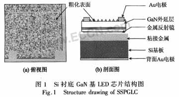
As seen from the structure diagram, the Si substrate chip is a flip-chip structure, and from the bottom to the top are a back Au electrode, a Si substrate, a bonding metal, a metal mirror (p ohmic electrode), a GaN epitaxial layer, a roughened surface, and Au electrode. The current distribution of the structure chip is vertical, the substrate has high thermal conductivity and high reliability; the back surface of the luminescent layer is a metal mirror, the surface has a roughened structure, and the light extraction efficiency is high.
1.3 Key technologies and innovation
The use of Si as a GaN light-emitting diode substrate has greatly reduced the manufacturing cost of LEDs and solved the patent monopoly problem. However, it is more difficult to grow GaN on Si substrates than sapphire and SiC. The thermal mismatch and lattice mismatch are larger, and the difference in thermal expansion coefficient between Si and GaN will also cause cracking of the GaN film. The difference in lattice constant will cause high dislocation density in the GaN epitaxial layer; It is also possible that a 0.5 V hetero barrier between Si and GaN causes an increase in the turn-on voltage and a poor crystal integrity, resulting in a low p-type doping efficiency, resulting in an increase in series resistance, and Si absorption of visible light reduces the outside of the LED. Quantum efficiency. Therefore, in view of the above problems, in-depth study and adoption of luminescent layer dislocation density control technology, chemical stripping substrate transfer technology, high reliability and high reflective characteristics of p-type GaN ohmic electrode preparation technology and bonding technology, high light extraction efficiency Material surface roughening technology, substrate patterning technology, and optimized vertical structure chip design technology have solved many technical problems in a large number of experiments and explorations, and finally successfully produced a light output of 1 mm × 1 mm and 350 mA. A blue light-emitting chip with a power of more than 380 mW, an emission wavelength of 451 nm, and an operating voltage of 3.2 V completes the specifications specified in the project. The key technologies and technological innovations adopted are as follows.
(1) Using a variety of on-line control techniques to reduce edge dislocations and screw dislocations in epitaxial materials, improve thermal mismatch and lattice mismatch between Si and GaN, and solve the problem of GaN single crystal films. For the cracking problem, a crack-free GaN epitaxial film having a thickness of more than 4 μm was obtained.
(2) By introducing AIN, AlGaN multi-layer buffer layer, the stress of the epitaxial GaN material on the Si substrate is greatly alleviated, the crystal quality is improved, and the luminous efficiency is improved.
(3) By optimizing the Si concentration structure in the n-GaN layer and the interface growth conditions between the quantum wells/barriers, the reverse leakage current of the chip is reduced and the antistatic performance of the chip is improved.
(4) By adjusting the p-type layer magnesium concentration structure, the operating voltage of the device is reduced; by optimizing the thickness of the p-type GaN, the light extraction efficiency of the chip is improved.
(5) By optimizing the epitaxial layer structure and doping profile, the series resistance is reduced, the operating voltage is reduced, the heat generation rate is reduced, the working efficiency of the LED is improved, and the reliability of the device is improved.
(6) Using a multi-layer metal structure, taking into account ohmic contact, reflective characteristics, bonding characteristics and reliability, optimizing the welding technology, solving the problem that the silver mirror and p-GaN are not firmly adhered and the contact resistance is large.
(7) A variety of soldering metals are preferred, the soldering conditions are optimized, and a strong bond between the GaN thin film and the conductive Si substrate is successfully obtained, and the crack problem generated in the process is solved.
(8) The surface roughening by the combination of the wet method and the dry method reduces the light loss caused by the internal total reflection and the waveguide effect, improves the external quantum efficiency of the LED, and enables the device to obtain a higher light extraction efficiency.
(9) Solved the problem that the GaN surface roughening depth is insufficient and the roughening is uneven, solves the problem that the rough surface cleaning is not clean and optimizes the metal structure of the N electrode, and obtains on the roughened N-polar n-GaN surface. Low resistance and stable ohmic contact.
2 Si substrate LED packaging technology
2.1 Technical route
The blue light LED is used to excite the YAG/silicate/nitrogen oxide multi-primary system phosphor, and emits yellow, green and red light, and synthesizes the white light.