For technical and economic reasons, MEMS sensors have been confined to the automotive market and industrial applications; today, as MEMS sensors become smaller and smaller, prices are getting lower and higher, energy efficiency is increasing, and design and application space is expanding. Its penetration rate in the consumer application market is constantly improving.
This article refers to the address: http://
The micromachining technology used to fabricate these devices is much the same as the process and process used to fabricate basic integrated circuits, except that micromachined products are typically a three-dimensional mechanical structure that can be moved (Figure 1).
While many different materials can be used to make MEMS products, silicon is gaining popularity in the industry because of its excellent electrical, mechanical, and thermal properties. In addition, semiconductor manufacturers are aware that tens of thousands of MEMS devices can be fabricated on a wafer once using proven chip manufacturing techniques. That is to say, MEMS can take advantage of the existing economies of scale of microelectronic devices and gain greater cost advantages, especially when entering the consumer products market, it is more important to take advantage of this advantage. Therefore, silicon is the most attractive MEMS material.
In the past, there were many applications that were impossible without this technology; today, this technology is making these applications possible.
Hard drive fall protection in laptops, mobile phones, portable media players and mobile devices is one of the most historic representative applications of MEMS motion sensors in the consumer electronics market.
The three-axis accelerometer in the laptop monitors acceleration because it has a specific function and data processing circuit that detects accidental drops from the hard drive and prompts the reader to retract to a safe position in case the computer The head was damaged when it fell to the floor.
Fitness and health monitoring are another representative application of MEMS sensors.
A pedometer or pedometer is a representative application for fitness and health monitoring using a three-axis MEMS sensor. In certain cases, the pedometer sensor accurately measures the action on the system during walking and running. Acceleration, by processing the acceleration data, the pedometer displays the number of steps and speed the user has traveled, as well as the amount of heat consumed during body movement.
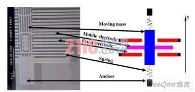
Figure 1: MEMS-based linear accelerometer.
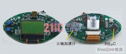
Figure 2: A MEMS-based pedometer reference design developed by STMicroelectronics.
The pedometer function is usually embedded in mobile phones and portable media players (MP3 and MP4). For these devices, you can set the number of steps to be achieved in a fixed time and measure the heat consumed to achieve this goal. . Members of the Virtual Gym can also share this information online and conduct virtual competitions that promote physical activity and fitness.
The pedometer is also an important module in portable navigation. The portable navigator is able to determine the user's location, provide routing functions, find public service locations, and receive regional advertisements. In special cases, for example, in the urban area, because the underground passage, overpass, high-rise, indoor block, the GPS signal will be weak, then the signal of the MEMS motion sensor can temporarily replace the GPS module, which plays a role in assisting navigation and positioning. .
In another application, MEMS sensors can be used to design an emergency device for the elderly. When the old man accidentally falls, the device can detect the fall action and automatically send an alarm signal to request emergency rescue. Through the MEMS sensor and GPS module, you can estimate the location of the injured elderly person who needs help and transmit the location information on the network. In the near future, the commercialization of these instruments will provide a safer living environment for a growing number of aging populations.
Today, MEMS sensors capable of detecting motion, direction and gestures are driving motion sensing technology to expand into markets such as mobile phones, game consoles, and portable media players.
With advanced features, compact appearance, and outstanding energy efficiency, MEMS sensors are enabling the introduction of more user-friendly devices. With these devices that recognize human gestures, users no longer have to read lengthy and complicated user manuals to learn how to use human-machine interfaces. .
MEMS helps break the barrier between users and applications: sensors like the eyes of the system can measure physical quantities such as acceleration and angular velocity; electronic components process the information sent by the sensors, use special algorithms to identify the input data, and then activate the corresponding functions. .
The game console is a prominent example of motion tracking and gesture recognition applications. Take the revolutionary Nintendo Wii console as an example. The miniature motion sensor captures any subtle movements of the player and turns them into action. MEMS technology allows players to move: the player is immersed in the real game experience and is integrated into the game through different actions, for example, imitating a real tennis match, a fascinating golf game, a tight boxing match or a relaxed fishing The action of the game (Figure 3).

Figure 3: MEMS moves the player.
The use of MEMS technology in mobile phones and PDAs is increasing, and more and more mobile phones using MEM accelerometers are currently on the market. The MEMS accelerometer in the mobile phone makes the human-machine interface simpler and more intuitive, and the interface function can be operated by the action of the hand, which fully enhances the user experience (see Figure 4).
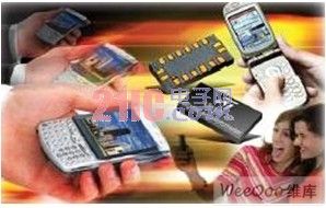
Figure 4: MEMS motion-controlled user interface.
Depending on the orientation of the terminal device, the MEMS sensor can rotate images, videos and web pages (whether portraits or landscapes). By tilting the phone up and down and left and right, you can also view the phone menu; just tap the phone body to select different icons on the screen, all of which are inseparable from the advanced digital technology embedded in the new generation of MEMS devices.
With the MEMS accelerometer, you can view the map in detail on a small screen and display the magnified image by tilting the device in a certain direction. MEMS can also detect the movement of the user's jittery phone and MP3 player. This simple gesture allows the player to jump to the next song or return to the previous song.
Low-power MEMS motion sensors can also be used as advanced energy-saving technologies. When the phone is not turned off and placed on the table, the MEMS sensor will turn off the power-hungry modules (such as the display backlight and GPS module) to reduce Energy consumption of mobile phones and portable navigation devices. Just touch the body and you can turn on all functions.
Similarly, whenever you put your phone face down on the table, the phone settings will switch to silent mode; you can turn off the mute function by touching the body. MEMS motion control technology reflects the look of the future of mobile phones: only a small number of buttons, no longer have a normal keyboard. When entering information into the phone, the user writes numbers and letters in the air, the MEMS sensor recognizes these actions, and the phone software restores these actions to numbers and letters; the software can also turn the user's predetermined actions into special custom functions.
MEMS accelerometers work with gyroscopes to turn more advanced selection features into reality, such as 3D mice and remote controls that can be operated in the air. In these devices, the sensor detects the user's gestures and converts them into cursor movements on the PC screen or channel and function selections for the set top box and the television. Figure 5 is a remote control solution with a MEMS sensor. The MEMS sensor group, two gyroscopes, and an accelerometer detect the motion of the wrist or mouse in the air, while the microcontroller performs motion tracking and gesture recognition. The recombined motion profile is then sent over a wireless connection to a set-top box or PC. The wireless link can be either infrared or radio frequency, depending on the application requirements.
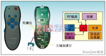
Figure 5: MEMS 3D remote control and indicator.
Recently introduced high-efficiency, low-cost miniature MEMS sensors have revolutionized the way people interact with mobile devices. On a variety of mobile terminals, game consoles, remote controls and other devices, MEMS motion sensors can achieve advanced functions, exciting user interface, user gestures, touches can activate the corresponding functions.
It is expected that in the near future, MEMS technology will be further developed, the surrounding environment will be filled with sensor networks, and our devices have embedded sensor networks, which will expand the space for feasible design applications, allowing us to better interact with the world. To better control the world we live in.
HDI PCB or High density interconnect PCBs are a way of making more room on your printed circuit board to make them more efficient and allow for faster transmission. It's relatively easy for most enterprising companies that are using printed circuit boards to see how this can benefit them.
High density interconnect (HDI) PCBs represent one of the fastest-growing segments of the printed circuit board market. Because of its higher circuitry density, the HDI PCB design can incorporate finer lines and spaces, smaller vias and capture pads, and higher connection pad densities. A high-density PCB features blind and buried vias and often contains microvias that are .006 in diameter or even less.
The copper is the circuits material and the circuits designed by the PCB designers. Depends on the current in the circuits, the PCB copper thickness could be done with 0.5oz-10oz. But the PCB designers need be noted that the copper track width/space need be enlarged with the thickness. For example, the minimum copper track width/space could be 3mil/3mil with 0.5oz, but would be 4mil/4mil with 1oz.
The PCB board could be rigid PCB, could be flex PCB and also could be Flex-Rigid PCB. And the materials could be FR4, PI, Aluminum, Copper-based, Rogers, Teflon, etc. They have different applications. For example, FR4 PCB is the most commonly used for rigid PCB and almost good for all electronics products; PI is the most commonly used for flex PCB; Aluminum and copper-based have good thermal diffusivity and always used for LED PCB ; Rogers PCB and Teflon PCB are always used for High Frequency PCB, etc.
PCB Manufacture Capabilities
|
Features |
Capabilities |
|
Layers |
1-36 layers |
|
Material |
FR-4, Aluminum, Copper, Polyimide, high frequency (Rogers, PTEE, PI), etc. |
|
PCB Type |
FR-4 Standard PCB , Aluminum PCB , Copper-based PCB, HDI PCB, Rigid-Flex PCB, Flex PCB, Thick Copper PCB and Rogers PCB, etc. |
|
Board Thickness |
0.1mm-6.0mm |
|
Copper Thickness |
1/2oz-6oz(18um-210um) |
|
Biggest Board size |
600mm*1200mm |
|
Min Tracing/Spacing |
0.075mm/0.075mm (3mil/3mil) |
|
Min drilling Hole diameter |
0.15mm(6mil), 0.1mm(4mil)-laser drill |
|
Solder Mask |
Green, Black, White, Red, Yellow, Blue and Purple, etc. |
|
Silkscreen color |
White, Blue, Black, Red, Yellow |
|
Surface finish |
HASL Lead free, Immersion Gold (ENIG), Immersion Tin, Immersion Silver, OSP, Carbon oil, etc. |
|
Special Techniques |
Impedance Control, Gold Fingers, Blind/Buried vias, Peelable solder mask, Half holes, Via-in-Pad and Countersink hole, etc. |
PCB Products Show

PCB Factory Show

HDI PCB
HDI PCB,HDI Microvia PCB,Prototype HDI PCB,HDI PCB Circuit Board
ZhongFeng Electronic Technology Co., Limited , http://www.dopcba.com