As semiconductor manufacturing capabilities allow the integration of thousands of gates on a single chip, system-on-chip (SoC) is beginning to dominate the future of IC technology. However, when people talk about SoCs today, they are actually talking about some systems—just integrating digital baseband with data converters, some high-speed analog IOs, and even some RF circuits, as long as it's not too complicated.
Due to process technology incompatibility, RF integration is often considered a largely unresolved SoC challenge. Integrating RF circuitry on digital dies can limit yield or lead to high test costs, which can significantly increase production costs.
But the problem is more complicated and subtle than this. From the perspective of SoC system, RF integration will bring some difficult development challenges to the circuit design, physical implementation and manufacturing and testing of hardware devices.
Now, RF chip designers have another option. Recent developments in CMOS manufacturing process technology have overcome RF integration barriers, allowing developers to move RF processing to the digital domain. Chip designers don't have to struggle to design and implement analog devices. Instead, they can use digital RF technology and use familiar tools and processes to process RF signals.
It is impossible to integrate only one type of radio
In order to adapt to the small form factor of a mobile phone or PDA, this requires simultaneous integration of digital, analog and RF on a single chip, otherwise the cost and form factor limitations will hinder the phone from configuring new functions. The integrated radio has only half the silicon area of ​​a conventional radio, occupies half of the board space and consumes about half of the power. Therefore, radio integration offers great advantages in meeting mobile phone design goals.
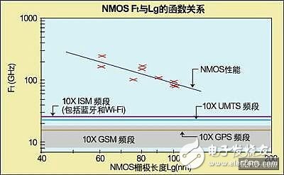
Figure 1: Tracking the cutoff frequency of each process node can evaluate these communications bands which can be processed in the digital domain.
Let's take a look at the data processing requirements of 3G mobile phones. In the digital domain, users want higher-resolution color screen displays, games that require additional memory and graphics resources, PDA application functions, and multimedia features such as photography, video conferencing, and audio playback. On the RF side, it is not unreasonable to integrate several types of radios in a mobile phone. They include:
* Many GSM phones support all four bands - cellular and DCS in Europe and different cellular frequencies and PCS in the US
* 2.1 GHz UMTS
* GPS for positioning and synchronization
* Bluetooth for PAN connection
* WiFi for network connection, if it is 2.4 GHz 802.11b/g, you can share Bluetooth radio
* Digital TV (DTV)
* Digital audio broadcasting and FM broadcasting, etc.
Today, the number of RF devices on the board is more than half of the total number of devices, and a simple radio takes up 40% of the area of ​​the printed circuit board (PCB). If you add radio to support features such as Bluetooth, GPS, and WLAN, these numbers are significantly increased. Although the radio can share some circuits, if they want to be loaded into a device, they must be smaller than they are today.
Problem
The practical problems encountered in integrating digital, analog, and RF circuits have poured cold water on those who are passionate about integrated silicon integration. For designs that integrate complex RF circuits on SoCs, there are still many areas for improvement in the available EDA development tools.
Tools for simultaneously verifying digital and RF circuits are still in the early stages of development, let alone verifying and testing designs. Other limitations include poor matching of small devices, high 1/f noise, and the lack of on-chip passive components (resistors, capacitors, and varactors) with sufficient analog features.
Despite these challenges, integration is still the basic means of reducing the cost, power, and complexity of radio designs for smartphones. In order to make radio integration a reality, the industry requires significant technological advances in wafer processing, system design, and circuit design. Although designers using SoCs are not concerned with many SoC technology challenges, it is important to understand these challenges as they determine the capabilities and limitations of the actual device. For example, while it is technically feasible to integrate RF using a bipolar or BiCMOS process, the yield limitations and high cost of testing devices do not necessarily enable high volume or commercial production of these devices.
Integrated silicon germanium (SiGe) BiCMOS technology is also possible. But silicon germanium technology is generally one or two process nodes behind advanced digital CMOS processes. Because mobile phones require more and more processing resources, the silicon germanium process cannot keep the die cost of the digital portion (especially memory) to a minimum.
Even CMOS RF integration has its challenges. The implementation of analog mixers, filters, and amplifiers is difficult, especially with voltage drops, and early device modeling of new process nodes is generally not sufficient to achieve the high-precision parametric modeling required for analog module design. The industry requires significant design innovations that allow the radio to be integrated into standard CMOS and take advantage of CMOS technology.
A different approach to digital RF integration to solve RF integration problems is to completely avoid them, which can be achieved by converting the functionality of the RF device to the digital domain.
By processing the RF signal in the CMOS digital domain, it is not necessary to use a complex and expensive analog mask. Chip design has also become easier because developers can more easily understand the system details during simulation and can perform processing by integrating programmable hardware and software elements to enhance control of the signal processing process.
For example, noise coupled from the power supply to the transmit and receive voltage controlled oscillators (VCOs) can affect overall system efficiency. Therefore, most wireless circuit board designs require regulators and associated passive components to solve this problem. Integrating these devices into a radio transceiver means that a simple decoupling capacitor is the only external component required to connect directly to the battery, simplifying design and saving board space.
Designers also have the option of integrating digital tuning and self-calibration into the VCO and integrating the loop filter to extend the tuning range of the VCO.
In order for digital circuits to process analog signals, they must operate at extremely high speeds. The device cutoff frequency (Ft) is a simple method used to evaluate the ability of a process to process RF signals (see Figure 1).
Small Pixel P2 Indoor LED Display, which include functions like High Resolution, High Refresh, High Definition. We Jongsun LED as specialized manufacturer, which focusing on the research and development, production, sales and engineering services of terminal P2 LED Displays. We have the perfectly after-sales and 7x24hours technical support. Looking forward your cooperation!
P2 Small Pixel,Led Display Screen Indoor,P2 Led Indoor Display,P2 Indoor Led Display
Shenzhen Jongsun Electronic Technology Co., Ltd. , https://www.jongsunled.com