DDR hardware design points
1. Power supply DDR power can be divided into three categories:
a main power supply VDD and VDDQ, the main power supply requirement is VDDQ = VDD, VDDQ is the power supply to the IO buffer, VDD is given but in general use VDDQ and VDD are combined into one power supply.
Some chips also have VDDL, which supplies power to the DLL and also uses the same power supply as VDD. When designing the power supply, it is necessary to consider whether the voltage, the current meets the requirements, the power-on sequence of the power supply, and the power-on time of the power supply, monotonicity, and the like. The power supply voltage requirements are generally within ±5%. The current needs to be calculated according to the different chips used, the number of chips, and the like. Since the current of DDR is generally large, if the PCB is designed to have a complete power plane laid on the pin, it is the most ideal state, and the capacitor is stored at the power inlet, and one pin is added to each pin. Small capacitor filtering from 100nF to 10nF.
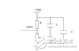
b Reference power supply Vref, reference power supply Vref is required to follow VDDQ, and Vref = VDDQ/2, so it can be provided by the power supply chip or by voltage divider. Because Vref generally has a small current, in the order of several mA~ tens of mA, the method of dividing the resistors, that is, cost saving, can be more flexible in layout, and is placed closer to the Vref pin, closely following VDDQ voltage, so this method is recommended. Need to pay attention to the voltage divider voltage can be used in 100~10K, you need to use 1% precision resistor. A 10nF point capacitance filter is required on each pin of the Vref reference voltage, and a capacitor is also connected in parallel with each voltage dividing resistor.
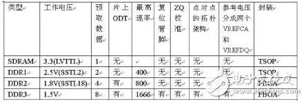
C, the voltage used for matching VTT (Tracking TerminaTIon Voltage)
VTT is the power supply to which the matching resistor is pulled up, VTT = VDDQ/2. In the design of DDR, depending on the topology, some designs use less than VTT, such as when the controller has fewer DDR devices. If VTT is used, the current requirement of VTT is relatively large, so it is necessary to use copper to spread the trace. And VTT requires the power supply to sink current and sink current. In general, a VTT-powered power chip designed for DDR can be used to meet the requirements.
Moreover, a capacitor of 10Nf~100nF is generally placed next to each resistor pulled to VTT, and a large capacitance of uF is required for energy storage on the entire VTT circuit.
In Huawei's design, in the case of using DDR particles, the VTT power supply has not been used at all, and all of the wearer-type pull-downs are used. The VTT power supply is used only when the memory stick is used.
In general, the data lines of DDR are all one-drive topology, and both DDR2 and DDR3 have ODTs for matching, so there is no need to pull to VTT for matching to get better signal quality. If the address and control signal line of DDR2 are multi-loaded, there will be more drives, and there is no ODT inside. The topology is T-type structure, so it is often necessary to use VTT for signal quality matching control. DDR3 can be routed in Fly-by mode:
A DDR3 design case to analyze and compare the difference between using a high-impedance load trace and using the main line and the load trace with the same impedance.
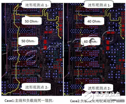
As shown above, Case1 uses a 50 ohm impedance design from the inner controller to each SDRAM. Case2 is designed with a main line of 40 ohms and a load line of 60 ohms. This is compared and analyzed by simulation tools.
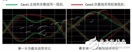
It can be seen from the above simulation waveform that Case2 using a higher impedance load trace is superior in signal quality to the case where the branch main line uses the same impedance of the Case1 design. Moreover, the load near the driving end is most affected, and the load at the far end from the driving end is less affected. This is exactly the previous analysis. The distributed capacitance of the load causes the impedance of the load line to decrease. If the main line and the load line are designed with the same impedance, the impedance discontinuity will occur. The load trace is designed to have a higher impedance, which is used to balance the distributed capacitance introduced by the load, so as to achieve the balance of the entire trace impedance.
The practice of balancing the load capacitance by increasing the load trace impedance is a method often used in previous daisy chain designs. DDR3 calls this topology fly-by, but it has a certain meaning, which is intended to emphasize that the load stub is short enough.
2. Clock
The DDR clock is a differential trace. Generally, the terminal is connected in parallel with 100 ohms. The differential trace differential pair has a control impedance of 100 ohms and a single-ended line of 50 ohms. It should be noted that the differential line can also use series matching. The advantage of using series matching is that it can control the rising edge of the differential signal, which may have a certain effect on EMI.
3. Data and DQS
The DQS signal is equivalent to the reference clock of the data signal, and it needs to remain the same length as the CLK signal when routing. DQS is a single-ended signal below DDR2. DDR2 can be used as a differential signal or as a single-ended terminal. DQS-grounding is required for single-ended, and DDR3 is a differential signal. A 100 ohm differential line is required. Since there is an ODT inside, DQS does not require a terminal to connect 100 ohm resistors in parallel. Each 8-bit data signal corresponds to a set of DQS signals.
The DQS signal needs to be the same length as the DQS signal of the same group when routing, and control the impedance of the single-ended 50 ohm. When writing data, DQ and DQS are aligned in the middle, and when reading data, the edges of DQ and DQS are aligned. The DQ signal is mostly one drive one, and DDR2 and DDR3 have internal ODT matching, so it is generally possible to perform series matching.
4. Address and control
The address and control signal speeds are not as fast as DQ, and are sampled on the rising edge of the clock, so they need to be equal to the clock trace. However, if multiple DDRs are used, the address and control signals are more than one drive. It is necessary to pay attention to whether the matching method is suitable.
Industry Pressure Transmitter,Pressure Transducer Sensor,Industrial Pressure Sensor,Electrical Pressure Transducer
Shenzhen Ever-smart Sensor Technology Co., LTD , https://www.fluhandy.com