Shareholder Xu Wei’s self-reliant portal and the original owner’s “snapping stationâ€
According to a “30t/a MO source project feasibility study report†provided by the insider, the company name is Anhui Yagesheng Electronic New Material Co., Ltd. (hereinafter referred to as “Yageshengâ€), Xu Wei, the shareholder of Nanda Optoelectronics Co., Ltd. It is the legal representative of the company. The reporter found Anhui Yagesheng Electronic New Material Co., Ltd. on the website of Wuhu Industry and Commerce Bureau. The company has a registered capital of 20 million yuan and its business scope includes research, development, production and sales of high-tech optoelectronics, photovoltaic and microelectronic materials. .
In this report, Yagsheng plans to implement a 30t/a MO source project with a total investment of 500 million yuan, and it is expected that Yagsheng will have a 40% market share in the domestic MO source market in 2013.
Although the legal representative of Yagsheng, Xu Wei, holds only 110,000 shares of Nanda Optoelectronics, he was a researcher at the MO Source Research and Development Center of the National Materials 863 Program of Nanjing University. According to the Nanda Optoelectronics Prospectus, Xu昕 “An important contribution to the research, development, formation and industrialization of this technology.â€
According to the disclosure of Nanda Optoelectronics' prospectus, Xu Wei, from August 1990 to 2000, worked at the National Source 863 Program New Material MO Source Research and Development Center of Nanjing University; from May 2011, he left from Nanjing University; November 2001-2006 In October, he served as assistant to the general manager and deputy general manager of the company. From April 2008 to present, he served as legal representative and general manager of Nanjing Yagetai New Energy Materials Co., Ltd.
In addition to being the deputy general manager of Nanda Optoelectronics, Xu Wei, in the non-patented technology independently developed by Nanda Optoelectronics and possessing independent intellectual property rights, the production, analysis and testing of trimethylgallium, control and packaging of MO source production processes, etc. The key technology, Xu Wei is an important research and development staff.
In this report, the 30t/a MO source project that Yagsheng plans to invest in is basically the same as Nanda Optoelectronics. Yagsheng said that "the project's trimethylgallium is synthesized by alloying method, purified by complex technology, and then subjected to precision fractionation. ICP-MS, ICP-OES, NMR, NMCVD, etc. are used for trace impurity analysis and application evaluation. After the product reaches the standard (≥99.9999%), it will be bottled for use."
In the prospectus of Nanda Optoelectronics, the company claims that the company's MO source is produced by a unique alloying method. In the MO source purification technology, it uses a unique complex purification and rectification technology. Moreover, the company has independent innovative sample decomposition technology. Advanced elemental impurity analysis using inductively coupled plasma optical emission spectroscopy (ICP-OES) and plasma mass spectrometry (ICP-MS)."
It can be seen that the company's core technology, production methods and production products are consistent with the investment projects of Nanda Optoelectronics. Despite leaving the company from Nanda Optoelectronics and still holding the shares of Nanda Optoelectronics, Xu Wei does not seem to intend to let the old-fashioned "cake" of the technology industrialization.
Interestingly, Yagsheng said in the report that the MO source produced by the company is an indispensable key raw material for manufacturing LED epitaxial chips, and its production technology is monopolized by a few companies around the world. These enterprises, based on their own interests, use monopoly positions to seek excess profits, and even cause a situation in the market where a “source†is hard to find, which seriously jeopardizes the healthy development of the LED industry.
Nanda Optoelectronics really do not know? Uninformed? Partnership wealth? In the prospectus of Nanda Optoelectronics, it was stated that the company was the only one in the country with independent intellectual property rights and realized the industrial production of MO source as of the end of the reporting period (meaning that the annual MO source capacity, production and sales volume reached more than 1 ton, and the quality is stable and reliable. The same as the company. In 2010, Nanda Optoelectronics has a global market share of approximately 15%, of which the domestic market share is above 60%.
At the same time, the high-purity metal organic compound industrialization project funded by Nanda Optoelectronics has completed the first phase of construction, with an investment of 37.83 million yuan. The investment of the raised funds is the second phase of the project, with a planned investment of 169,883,200 yuan. The new production capacity after the production is 22.5 tons.
At this time, the first phase of the project has also started. From 2011 to 2012, Yagsheng invested RMB 170 million through the shareholders' self-raising and bank loan program to realize the MO source capacity of 10 tons. In 2013, Yagsheng will have a 40% market share in the MO source market.
It can be seen that Yagsheng, founded by shareholder Xu Wei, will become a strong rival of Nanda Optoelectronics in the MO source market. Is Nanda Optoelectronics Management really ignorant of this? And Nanda Optoelectronics is in the prospectus for Xu There is very little ink in the eyes, and it seems to be deliberately concealed.
Yagsheng also said in the report that it will complete the listing financing in 2013. Although the current composition of the equity of Yagsheng is still unclear, as the core personnel of Nanda Optoelectronics, is there any old company to contribute money behind it? There is something unspeakable between Yagsheng and Yagsheng, so stay tuned for follow-up development.

Multi-layer PCB is the printed circuit board that the copper layer equal or beyond 4layer. For example, we could do 1-36layer PCB, so 4-36layer PCB are all Multilayer PCB. For multilayer PCB, the copper thickness of each layer could be same and also could be different, it's based on the layer stack-up. And normally, multilayer PCB may require impedance control.
How Are Multilayer PCBs Made?
Alternating layers of prepeg and core materials are laminated together under high temperature and pressure to produce Multilayer PCBs. This process ensures that air isn't trapped between layers, conductors are completely encapsulated by resin, and the adhesive that holds the layers together are properly melted and cured. The range of material combinations is extensive from basic epoxy glass to exotic ceramic or Teflon materials. The figure above illustrates the stackup of a 4Layer/ multilayer PCB. Prepeg and core are essentially the same material, but prepeg is not fully cured, making it more malleable than the core.The alternating layers are then placed into a lamination press. Extremely high temperatures and pressures are applied to the stackup, causing the prepeg to "melt" and join the layers together. After cooling off, the end result is a very hard and solid multilayer board.
-Higher assembly density
-Smaller size (considerable savings on space)
-Increased flexibility
-Easier incorporation controlled impedance features.
-EMI shielding through careful placement of power and ground layers.
-Reduces the need for interconnection wiring harnesses (reduces overall weight)
PCB Manufacture Capabilities
|
Features |
Capabilities |
|
Layers |
1-36 layers |
|
Material |
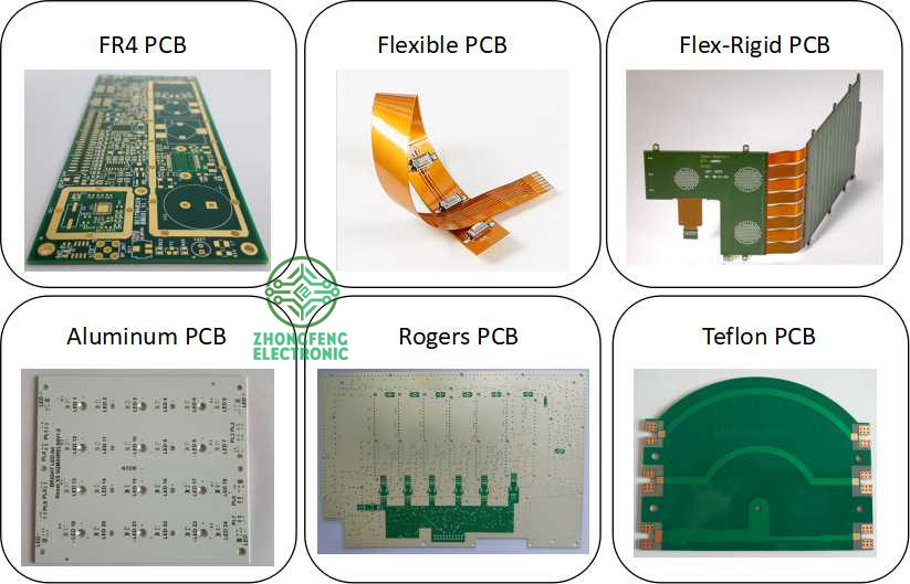
FR-4, Aluminum, Copper, Polyimide, high frequency (Rogers, PTEE, PI), etc. |
|
PCB Type |
FR-4 Standard PCB, Aluminum PCB , Copper-based PCB, HDI PCB , Rigid-Flex PCB, Flex PCB, Thick Copper PCB and Rogers PCB, etc. |
|
Board Thickness |
0.1mm-6.0mm |
|
Copper Thickness |
1/2oz-6oz(18um-210um) |
|
Biggest Board size |
600mm*1200mm |
|
Min Tracing/Spacing |
0.075mm/0.075mm (3mil/3mil) |
|
Min drilling Hole diameter |
0.15mm(6mil), 0.1mm(4mil)-laser drill |
|
Solder Mask |
Green, Black, White, Red, Yellow, Blue and Purple, etc. |
|
Silkscreen color |
White, Blue, Black, Red, Yellow |
|
Surface finish |
HASL Lead free, Immersion Gold (ENIG), Immersion Tin, Immersion Silver, OSP, Carbon oil, etc. |
|
Special Techniques |
Impedance Control, Gold Fingers, Blind/Buried vias, Peelable solder mask, Half holes, Via-in-Pad and Countersink hole, etc. |
PCB Products Show

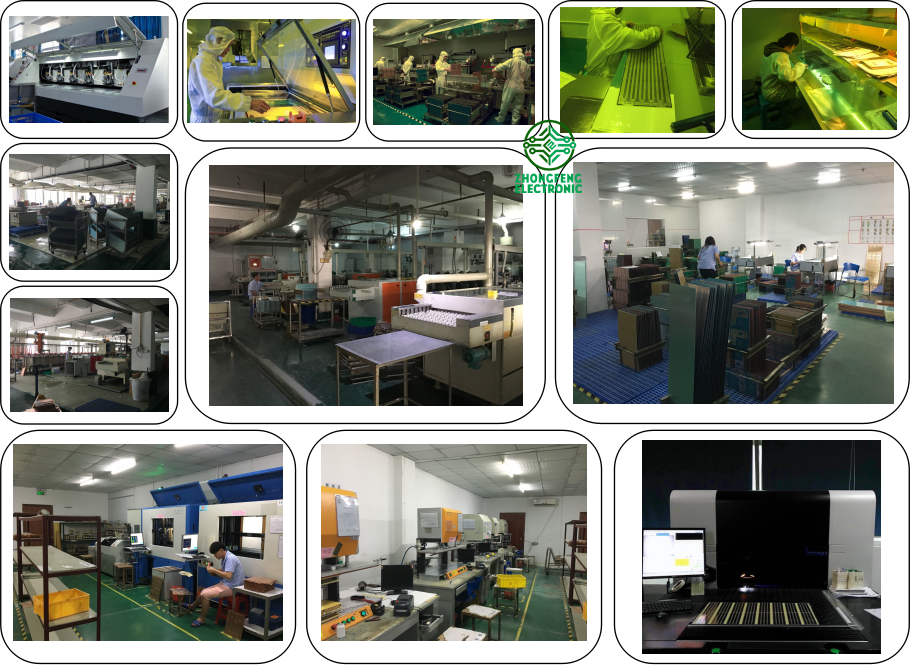
PCB Factory Show

Multilayer PCB
Multilayer PCB,Multilayer PCB Board,Multilayer PCB Design,Multilayer PCB Prototyping
ZhongFeng Electronic Technology Co., Limited , https://www.dopcba.com