Since July 13, NVC Lighting Headquarters, Chongqing Wanzhou Factory and Guangdong Huizhou Factory have successive strikes, demanding the return of Wu Changjiang. NVC Lighting spokesman Shi Yongjun said on the 27th that Wanzhou, Chongqing and Huizhou have resumed their work today.
Shi Yongjun said that the decision to return to work was not from the joint decision of Yan Yan and the board of directors, but the result of in-depth communication between Vice President Mu Yu and the middle management of the three places. Mu Yu is currently the vice president of NVC Lighting, the only executive director of the board of directors, and has been working with Ng Changjiang for 12 years at NVC.
The reporter verified from the administrative department of Wanzhou NVC, and after receiving the notice of resuming work, "the roar of the machine has been heard on the production floor on the 27th." A person in charge of the anonymous Southwest Operation Center said that on the morning of the 27th, the operators I have already received the news of the return of work, "the factory said that it can accept the order." However, the reporter found that some operators did not participate in the new brand meeting. In a small conference room on the fourth floor of the Yihao Hotel in Zhongshan International Trade, dozens of people were also scattered.
"We hope that when a finished product appears, it will be announced. It is not a good time to say it." When the reporter was found, a responsible person invited the reporter out of the meeting.
The reason for the absence of the operator in a certain area in the northwest of NVC is: "The few people who have to take the lead in any case have the final say, it doesn't matter if they go." The newspaper confirmed that the NVC dealers are the leader of the self-reliant portal. Including Li Guanyu, general manager of Yunnan Operations Center, Zhou Guangquan, general manager of Heilongjiang Operation Center, and Wu Xiaolin, general manager of Shaanxi Operations Center.
Previously, all three had informed the outside world that a new lighting company would be established. It is understood that the new company registered capital of 50 million yuan, the company headquarters will be located in Chongqing, Guangdong Zhongshan as a production base. At present, the dealers have raised 300 million yuan for the new company and prepared funds of 1 billion yuan, and stressed that "36 dealers and 40 suppliers jointly participated." However, NVC Lighting Management did not attend the meeting. The above-mentioned southwestern operator said to reporters on the 25th: "Everyone (operator) has feelings for NVC lighting, but if the core interests are not met, then they have to make plans for themselves."
The core interest of the operator refers to the four-point appeal put forward on July 17: Wu Changjiang re-elected as chairman and executive director; replaced the personnel sent by the existing management Schneider side; appointed management and distributor representatives as Additional directors of the company; giving management and core personnel options. The first two are considered to be the core of this NVC infighting.
"If Wu Changjiang can't return to NVC, NVC's 36 operations centers and 3,000 specialty stores can remove NVC's trademark overnight and replace it with a new one." Heilongjiang operators once told the media. It is understood that the middle management of NVC also rushed to Chongqing to meet on the 27th.
The board of directors held on July 25 was considered to be the key battle of Wu Changjiang's return to NVC, but the meeting was still unable to reach a resolution on the 26th. People close to Saifu revealed that Wu Changjiang’s return to NVC could not be concluded in the near future. In fact, since May 25, Wu Changjiang resigned as chairman, executive director and chief executive officer due to physical reasons, NVC Lighting's share price fell more than 40% before the company's suspension.

4 Layer PCB
What is 4 layer PCB?
Four-layer circuit board is a kind of Printed Circuit Board. It is made of four layers of glass fibre, which can reduce the cost of PCB.
Compared with Double Sided PCB , multi-layer PCB have many advantages. They can be designed more compactly. They can greatly improve noise resistance and make layout easier.
There are also great differences between the 2-layer and 4-layer PCB. For details, please click: What's the difference between 2 layer and 4 layer PCBs?
4 layer PCB stackup and thickness

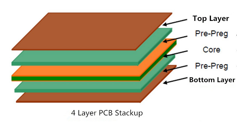
4 layer PCB stackup include two inner layers, inner layer 1 and 2, are sandwiched between the top and bottom layers. From top to bottom, the 4-layer PCB stackup like below ,The top, i.e. the signal layer (0.0014 in. width) is followed by a prepreg layer with a thickness of 0.0091 in. and dielectric constant of 4.2. The top layer is copper material. The prepreg layer is followed by inner layer 1 (0.0014 in.), referred to as the plane. A core sublayer is part of inner layer 1, which has a width of 0.037 in. This is followed by inner layer 2, which is another plane layer made with 1 oz. copper and is 0.0014 in. thick. Another prepreg sublayer constituting two sheets that are 0.0091 in. thick forms part of inner layer 2. The final layer, the bottom layer, is also 0.0014 in. thick, and is a signal layer as well. Interconnects are soldered and placed on the top and bottom layers.
4-layer PCB has two stacking forms
The standard 4-layer PCB stack is shown below, and GND and VCC can be switched according to the layer with more signals.
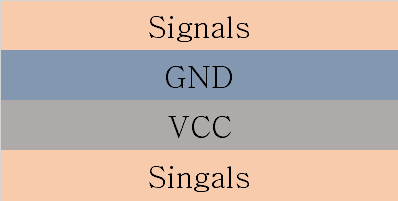
If you don't want to connect all the ground pins through the hole, there will be different stacks and wide power routing on the signal plane.
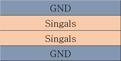
For the following reasons, this may be a better stack to use a four-layer PCB:
- The signal layer is adjacent to the plane. The signal running on the reference plane (whose voltage is exactly at the VCC) will still return on the reference plane.
- Signal layers are tightly coupled to their adjacent planes.
- The ground surface can be used as a shield for the internal signal layer. You will get better results, so that your plane height is as low as possible.
- Multiple grounding layers reduce the grounding (reference plane) impedance of PCB and common mode radiation.
When the high-speed signal changes the reference plane, there should be a nearby path for its return current to move between the two reference planes. Using two horizons, you can do this by connecting two planes directly to a single channel. For grounding and power layers, the connection must be made through capacitors, which usually require two through-holes and one capacitor. This means worse signal integrity and more circuit board occupancy. On the other hand, having a power plane can reduce the voltage drop on the power rail, thereby releasing the space on the signal layer.
PCB Board Thickness
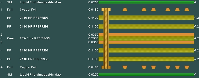
4 LAYER 0.8 MM STANDARD BUILD
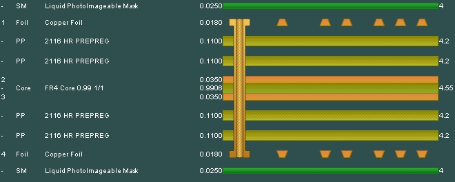
4 LAYER 1.6 MM STANDARD BUILD
0.4mm, 0.6mm, 0.8mm, 1.0mm, 1.2mm, 1.6mm, 2.0mm, 2.4mm, Please contact us if your board exceeds these.
4 layer PCB Prototype
4-layer circuit board prototyping refers to the trial production of Printed Circuit Boards before mass production. It is mainly used for electronic engineers to design circuits and complete PCB Layout, then to carry out small-scale trial production process to the factory, that is, proofing PCB. The production quantity of four-ply proofing generally has no specific boundaries. Generally, engineers call it proofing before product design has not been confirmed and test has been completed.
Notices for proofing of four-layer circuit boards
The precautions for the production of four-layer PCB samples generally include two groups, one is the Engineer group, the other is the PCB Sample manufacturer.
As a group of engineers, the matters needing attention in proofing are as follows:
1. Choose proofing quantity carefully to control cost effectively.
2. Specially confirm device packaging to avoid proofing failure due to packaging errors.
3. Conduct comprehensive electrical inspection to improve the electrical performance of PCB board.
4. Make good signal integrity layout, reduce noise and improve PCB stability.
As a manufacturer of four-layer circuit boards, the precautions are as follows:
1. Check PCB files carefully to avoid data problems.
2. Conduct process approval in an all-round way and process configuration with self-manufacturer.
3. Control production quantity, reduce cost and maintain quality.
4. Communicate with customers who need samples to prevent accidents in advance.
4 layer PCB price and cost
We specialize in Quick Turn PCB services with an industry leading turnaround time as fast as 24 hours. Three low-cost options for a small number of PCB prototyping needs. At the same time, we also provided Flexible PCB , Rigid- Flex PCB , Metal Core PCB , High-TG PCB, Aluminum PCB , PCB Stencils, PCB Assembly Services and so on. Using the same high-tech equipment as our full-service PCB, it can be manufactured quickly and with virtually no limits.
Cost of four layer PCB is higher than double sided PCB because of complexity of design and higher sensitivity. The better quality of signals, achieved by reducing distortion and propagation levels, is also a factor. Because of the higher levels of signal integrity and reduced interference levels, more manufacturers prefer four layer PCB.
4 layer PCB Manufacturing
We provide a full range of PCB functions to meet all your PCB needs. At present, we accept five PCB file formats (gerber file,.Pcb,.Pcbdoc.cam or.brd file format) for PCB manufacturing. But if you design a circuit board using Sprint-Layout software, you can send the. LAy6 file to us to manually generate the Gerber file.
JingHongyi PCB can provide you with multi-layer PCB board that meets RoHS standard. With laminated material, it can match high temperature in assembly process. It is important to remember that some lead-free assembly processes will require laminated substrates to withstand temperatures exceeding 260 degrees Celsius or 500 degrees Fahrenheit over a longer period of time. To solve this problem, we have high temperature laminates in stock, so that our customers can meet the higher temperature cycle requirements of some lead-free assembly applications.
Min. Order Quantity: 1 pcs
Material: FR-4
Finished Copper: 1oz/2oz/3oz(35μm/70μm/105μm)
Inner Layer Copper Thickness:1oz/1.5oz(35μm/50μm)
Silkscreen: White, Black, None
Surface Finishing: HASL with lead, HASL lead free, Immersion gold, Hard Gold ,OSP...
Shape: Custom Shape
100% Quality control
When making circuit boards, and after they are finished, we will test and inspect them strictly to ensure that the product reaches 100% eligibility rate. Preferential prices and higher quality have always been our constant pursuit:
- E-test
- AOI - Testing (Automatic Optical Detection)
- X-ray (check multi-layer registration accuracy)
- CCD-camera controlled drilling
- Impedance control
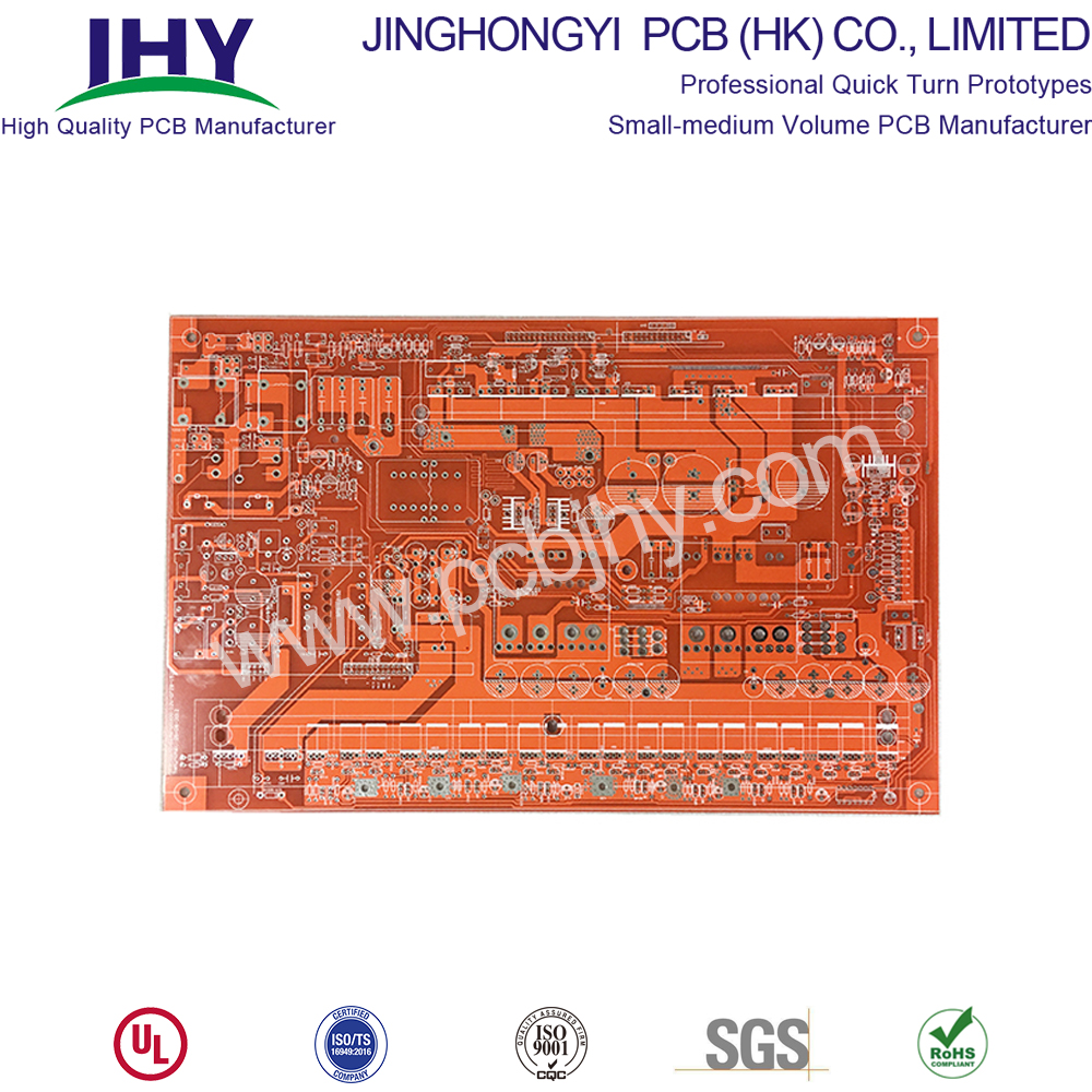
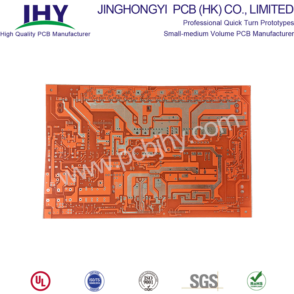
Videos for 4 layer PCB design and manufacturing
4 Layer PCB
Printed Circuit Board,4 Layer PCB,4 Layer PCB Board,4 Layer Printed Circuit Board
JingHongYi PCB (HK) Co., Limited , https://www.pcbjhy.com