Introduction
With the advancement and development of digital technology, high requirements have been placed on the high rate and timeliness of data transmission. The emergence of the IEEE1394 protocol has solved this problem well. IEEE1394, also known as FIReWire, is a high-speed serial bus that has developed IEEE1394b to provide rates up to 3.2 Gb / s and extends the transmission distance to 100 m. It can be concluded from this that 1394 will inevitably become the "standard" serial bus of the future.
IEEE1394 supports 2 types of transactions: isochronous transmission and asynchronous transmission.
Asynchronous transmission (asynchrONous transacTIons) ensures the accuracy of data transmission, but does not guarantee the timeliness of data transmission. It is mainly used to transmit control information and some data that requires high data accuracy. An asynchronous transmission consists of 4 parts: request packet, request confirmation packet, response packet and response confirmation packet. The confirmation data packet is synchronized with the request data packet and the response data packet. When the request data packet and the response data packet are sent, it is the confirmation data packet immediately.
Asynchronous transmission does not occupy a fixed bandwidth, but it can ensure that the nodes obtain fair access in time, and each node that performs asynchronous transmission can accurately access the bus within a single interval.
Isochronous transmission (isochronous transacTIons) has high requirements for the timeliness of data transmission, while the requirements for the accuracy of data transmission are relatively low. Isochronous transmission uses a channel number determination device associated with isochronous transmission, which sends data at a fixed time interval (125 μs), so a fixed bus bandwidth must be allocated, which has a higher priority than asynchronous transmission, and isochronous transmission is available. The maximum bandwidth is 80% of the entire bandwidth.
According to the structure of the protocol, the 1394 protocol can be divided into a transaction layer, a link layer, a physical layer, and a bus management layer. The link layer and the physical layer are currently implemented by hardware chips. This design is mainly for the application of the chip, so there is not much introduction and research on the protocol itself.
2 Acquisition system hardware design
According to the characteristics of the hardware, a CCD camera acquisition system based on T1 chipset and FPGA is designed. The system structure is shown in Figure 1.
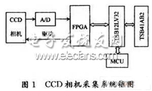
FPGA selects Altera's Cyclone series device EP1C6T144C8, which can provide the driving timing required for the CCD camera to work, and at the same time receive the A / D converted CCD output image data.
Here mainly introduces the data collection of the 1394 interface, and the CCD drive logic inside the FPGA is temporarily not introduced. This design is used for the transmission of large amounts of data, so the DM port of TSB12LV32 is used to input and output data. The logic circuit of DM port of FPGA and TSB12LV32 is shown as in Fig. 2.

An asynchronous FIFO is used inside the FPGA to solve the problem that the CCD output data frequency and the TSB12LV32 acquisition frequency do not match. The write clock is provided by the CCD output bit synchronization signal, and the write request signal is jointly controlled by the full state of the FIFO; the read clock is provided by the DMCLK of the TSB12LV32, the read request The signal is from DMRW. When TSB12LV32 starts to transmit data, under the control of the full state of FIFO and the DMDONE pin of TSB12LV32, the data is written into the FIFO by the CCD output bit synchronization signal; under the control of DMWR, the data in the FIFO is changed from DM0 to DM7 The pin reads in TSB12LV32, the connection is shown as in Fig. 2.
2.1 MCU software design
The design of the software is divided into 2 parts: one is to develop the driver of the device board on the PC; the other is to use the MCU on the device board to control and configure the software process of the PDI1394L40. The single chip is mainly responsible for initializing each CRF, setting the working mode of TSB12LV32, configuring the ROM to send the ROM, analyzing the packet header, constructing the packet header and the data packet. The configuration ROM is the focus of the design and the difficulty. Insert the device into the 1394 port of the PC. Through the configuration ROM, the PC can recognize the device. The process of configuring ROM is shown in Figure 3.

Cat 6 Connectors,Cat6A Connectors,Cat6 Utp Connector,Cat6 Utp Plug
Dongguan Fangbei Electronic Co.,Ltd , https://www.connectorfb.com