Since UV LED is a semiconductor component that integrates heat and light, it is necessary to consider the influence of related characteristics on its function and life in the R&D and manufacturing of components and the application and design of components. Through the following cases, we can further understand its characteristics.
Conjecture brought by the case
The following figure shows the phenomenon that a system manufacturer uses a water-cooled system for a period of time (two months) under the condition of 700 mA current. The phenomenon of lamp bead discoloration is obvious in the figure. Why is this happening? ? Everyone thinks that there should be a problem with heat dissipation. On the surface, the surface of the chip turns yellow. Is that really the case?
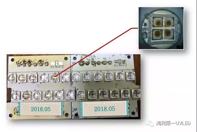
Figure 1: Bad samples
Verification of conjecture
In order to find the real reason, we analyzed and dissected this defective product to determine the cause of the true discoloration.
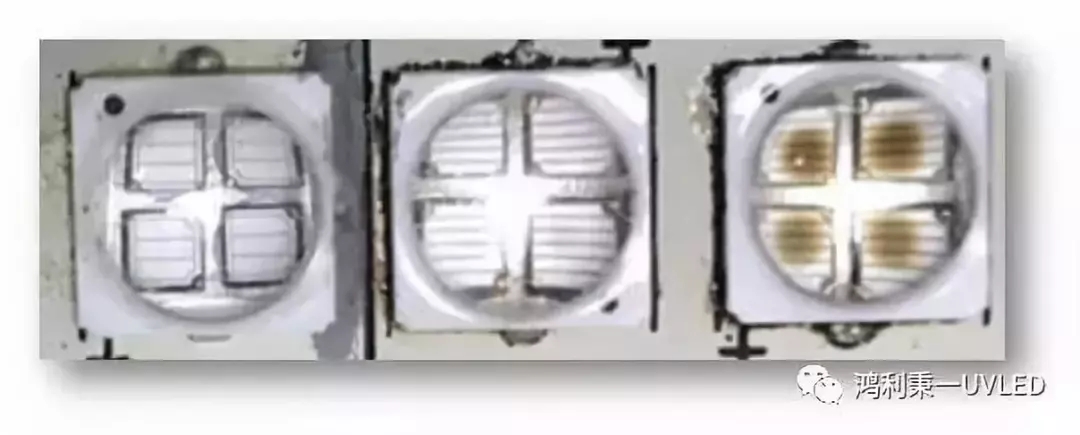
Figure 2: Chip View
From the above figure, we can clearly see that the chips used in the two sets of modules are completely different in appearance. From this we can understand that different manufacturers or products of different periods are placed in the same system, by querying two chips. They are all chips from the same manufacturer, but the chips have been improved. The improvement of the chip process will involve related changes in photoelectric characteristics. When the chips under different processes are put together for product design, the photoelectric parameters may not be caused. Matching, which affects the thermal performance imbalance of the product.
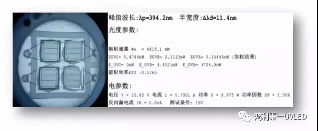
Figure 3: Lamp Bead 1 Photoelectric Test Data
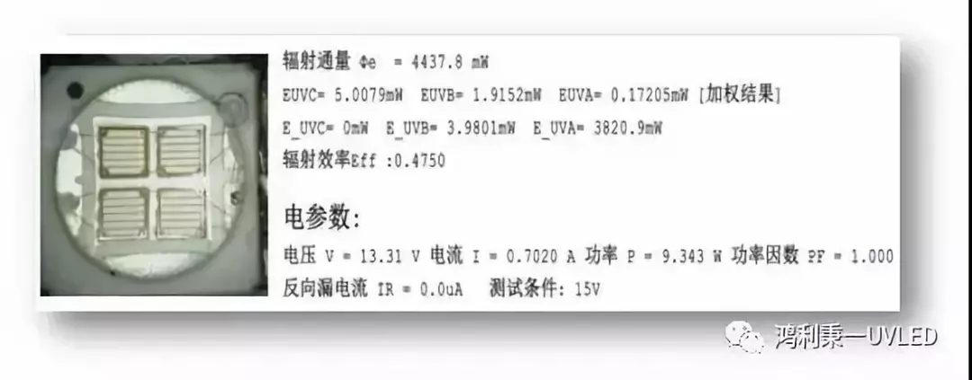
Figure 4: Lamp 2 Photoelectric Test Data
From the above photoelectric parameter analysis, the parameters under the two processes are slightly different. The voltage of the lamp bead 1 is 12.82V, and the voltage of the lamp bead 2 is 13.31V. According to our 0.4V pitch standard, the voltage range is too wide. Can not be used together. From the perspective of the radiation efficiency of the lamp bead, the lamp bead 2 is smaller than the lamp bead 1, indicating that more electric energy is converted into heat energy.
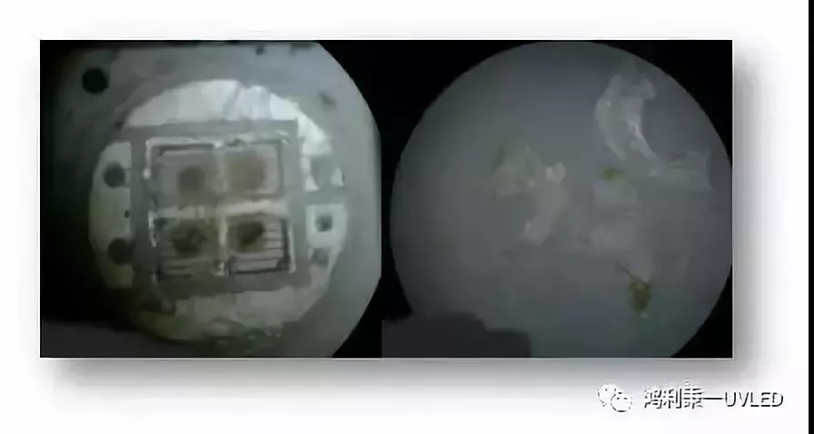
Figure 5: Rear view after lens removal
The picture above is the picture after removing the glass lens. It is easy to see from the figure that the packaging process is to apply a glass lens after coating the surface of the chip. This packaging process is the production process of visible light LED, because the glass lens is glued. The way, the inherent airtightness is poor, in order to protect the chip, gold wire and cavity from harmful substances, the surface of the chip is coated with a kind of silica gel for protection. In the figure, we can also see the colloid or The chip has traces of discoloration. So is it a colloidal discoloration or a chip discoloration?
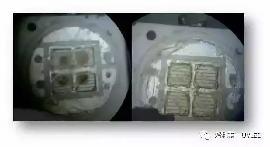
Figure 6: Comparison chart before and after degumming
After removing the colloid on the surface of the chip, we found that there is no yellowing on the surface of the chip, so it can be confirmed that the yellowing substance is actually the colloid itself.
For colloidal yellowing, we will consider the problem of heat dissipation. The heat conduction will not go out. This phenomenon will occur after a certain period of time. This is a common problem in high-power white light packaging. To further analyze the thermal conductivity of the package, we tested the void ratio of the solder layer under the X-Ray device.
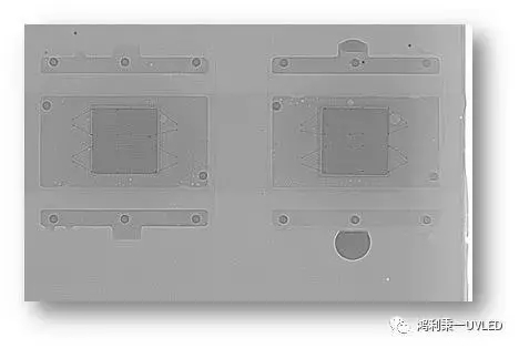
Figure 7: Cavity rate detection
Moreover, as can be seen from Figure 1, the defective products in the two modules are all concentrated on one module. If the heat dissipation is not good, the defect should not be on only one board. Is this the two processes mentioned above? Why are the chips put together? Is this the real reason? It can be seen from Fig. 7 that the welding void ratio is within 15%, which is very good in the soldering process. Is the heat generated by the chip itself not conducted out?
Below we analyze the heat dissipation capability of the lamp beads corresponding to the two chips to analyze whether the glue is discolored due to different chip processes.
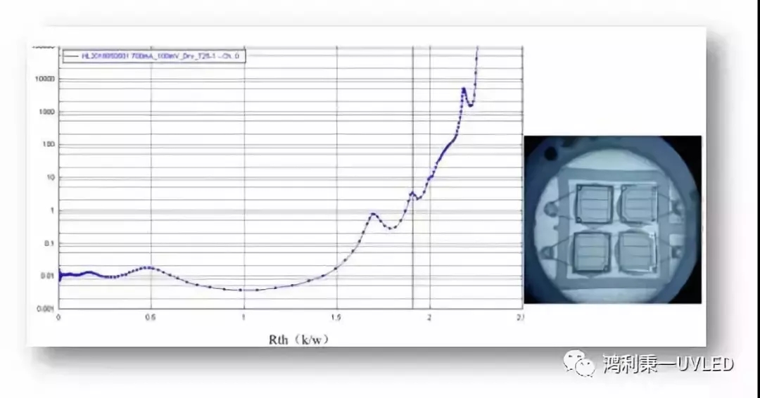
Figure 8: Lamp 1 thermal resistance test curve
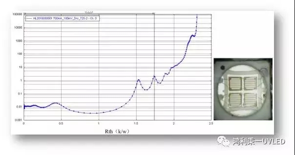
Figure 9: Lamp 2 thermal resistance test curve
From Fig. 8 and Fig. 9, we can understand that the thermal resistance of lamp bead 1 and lamp bead 2 are less than 2K/W. This thermal resistance reflects that the lamp bead itself has good thermal conductivity, and the thermal conductivity of the two bead is equivalent. That is to say, the discoloration of the lamp bead is not caused by the different chip processes.
The following is to analyze the characteristics of the glue. Generally, the current power-type package will use organic silica gel, while the organic silica gel has methyl silica gel and phenyl silica gel. The moisture permeability of methyl silica gel is 20,000 to 30000 cm3/(m2). ×24H×atm), the moisture permeability of phenyl silica gel is 300-3000cm3/(m2×24H×atm), and generally gas and water can penetrate into the interior of the organic silica gel, and the moisture permeability of the packaging material is high. The airtightness of the device is poor, and harmful substances in the external environment are easily invaded into the device through the package material, resulting in device failure. It has been found that organic materials are photodegraded by UV light for a long time (photooxidation occurs in an aerobic environment) [1], aging and yellowing occur [2], and severe cracking even occurs [3], making the device A significant drop in light extraction efficiency and reliability ultimately leads to failure, a phenomenon that is particularly severe in the deep ultraviolet range. Through the analysis of the characteristics of the glue, we should be aware of the reasons for the phenomenon of colloidal yellowing, that is, the poor airtightness of the glue, the invasion of air and moisture, and the yellowing that occurs under the action of UV light, so why is the same On the system, does this phenomenon only appear on a chip? This is the chip produced by different processes mentioned above, the photoelectric parameters are different, which affects the different thermal environment of the colloid, and the yellowing time is different, but the packaging of the organic UV LED is also used after a period of use. Colloidal yellowing will occur. So how to avoid such problems?
Case tells us how to choose UV LED package structure
The all-inorganic package adopted by Hongli Bingyi is ceramic C+metal M+hard glass H. There is no organic material in the whole packaging process, and glass is a kind of high-quality inorganic substance with intermolecular gap smaller than water, so generally Gas and water are not transparent to the glass, so glass is easier to achieve a hermetic package than silicone.
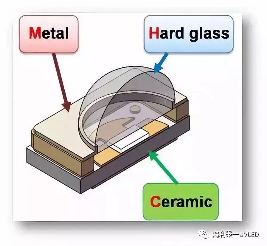
Figure 10: CMH package structure
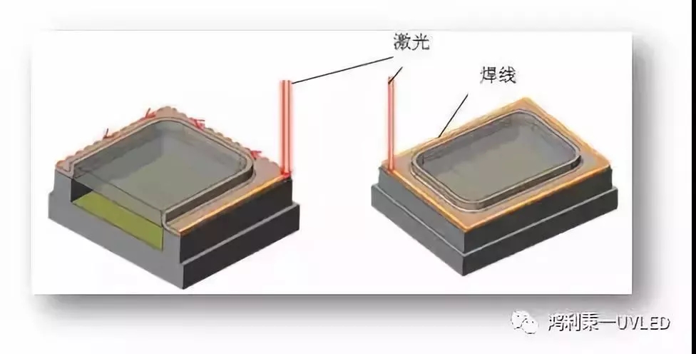
Figure 11: Sealing diagram
The process can be hermetically sealed by laser welding in a vacuum or dry protective atmosphere, and the airtightness can meet the requirements of the US military standard MIL-STD-883. It can provide a relatively low-oxygen, dry and relatively stable use environment for the chip, and has better UV resistance than organic materials, thus ensuring long-term use of UV LED without performance degradation due to the inclusion of machine packaging materials. For industrial applications, the light source is a key component, so the requirements are relatively high. To ensure the reliability of the application, I believe that the package mode of the all-inorganic UV LED is the best choice.

TV Antenna ,HDTV Antenna ,TV Antenna Best ,TV Antenna Walmart ,TV Antenna digital
Yetnorson Antenna Co., Ltd. , https://www.yetnorson.com