With the development of China's aviation industry, more and more aircraft designed by China are flying in the sky. In order to record the parameters of various aircraft equipment during the flight of the monitoring aircraft, the flight parameter recording instrument is required for real-time recording. There are many types of equipment, interface types and signal types on the aircraft. In order to meet the needs of various aircraft models, the size of the flight parameter collector equipment needs to be relatively small, so that both large aircraft and small aircraft can be used.
In order to meet the above requirements, the best way to use is to use a chip with multiple functional modules for development and design, so as to avoid the use of multiple separate functional chip designs, resulting in excessive device size and poor system coordination. Happening. The S698-T chip is a 32-bit RISC integer unit based on SPARC V8 (IEEE-1754) architecture developed by Zhuhai Oubit Control Engineering Co., Ltd., which is a 64-bit dual with IEEE-754 standard. Precision floating point processing unit FPΜ. High-performance, high-reliability, high-integration embedded SoC chips in the BGA352 package fabricated and fabricated in a 130 nm CMOS process. The S698-T also integrates 1553B bus controller, ARINC429 bus controller, CAN bus controller, multi-function IO interface, ΜART interface, online hardware debugging support unit DSΜ, DAC module, ADC module and other functional modules.
1 Flying gin collector hardware design
The main function of the flying ginseng collector is to complete the high-precision acquisition of the input channel parameters and output it to the recorder according to a certain format; connect the host computer through the Ethernet interface to complete the functions of parameter configuration, history setting, data calibration, data unloading, etc. The collector has a real-time clock inside, and the collected result data has clock information; it has 8 high-speed sampling channels. These 8 channels can be used as virtual oscilloscopes in debug mode. In the acquisition mode, signals can be collected normally. The CAN bus can be cascaded to expand the acquisition channel; the product supports power-on self-test, cycle self-test and maintenance self-test, and can record and report self-test information to facilitate fault location; products consider EMI, EMC design, improve product resistance Electromagnetic interference capability.
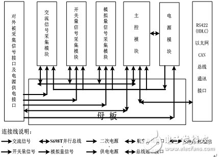
The collector is modular in design and its overall block diagram is shown in Figure 1. The collector consists of six parts: power module, main control module, switch signal acquisition module, analog signal acquisition module, AC signal acquisition module, and motherboard.

Figure 1 Product block diagram
The power module mainly implements DC-DC power conversion to provide stable power for other functional modules in the product.
The main control module integrates the system controller, aviation bus interface (including 1553B bus interface, ARINC429 bus interface, CAN bus interface, RS422 interface, RS232 bus interface, Ethernet bus interface) and onboard cache and other modules.
The switch signal acquisition module mainly completes the acquisition of 90-way switch signals.
The analog signal acquisition module mainly completes 5 fuel consumption signals, 5 0-100 mV analog signals, 5-10-10V DC differential signals, 30 ±35 V DC signals, 10 ±200 V DC signals, and 8 channels. High-speed sampling function, 8-channel frequency signal and 10-channel current ratio meter acquisition.
The AC signal acquisition module mainly performs the acquisition of 6 36-380 V AC analog signals and 6 3-phase AC synchronizer signals.
The collector adopts modular design. In addition to the power module, the main control module directly controls the other three functional modules through the parallel bus. All parameter configurations, the collection result data frame combination are completed on the main control board, and the main control board provides Ethernet. The interface is used for communication with the host computer, performs parameter configuration, analyzes and checks data acquisition during acquisition, and uploads data of the high-speed acquisition channel, and provides an RS422 interface for transmitting the collected result data to the recorder.
The motherboard is mainly used to implement the connection between the external interface and each functional module and the interconnection between the functional modules.
2 FPGA design implementation
There are 4 functional modules in the collector that relate to the FPGA design.
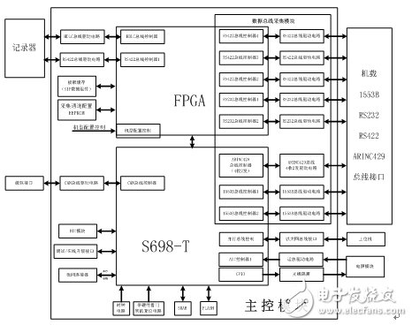
The functional block diagram of the main control module is shown in Figure 2:

Figure 2 Functional block diagram of the main control module
The FPGA of the main control module mainly implements the following functional modules:
2 1-channel HDLC bus interface controller, requiring a transmit FIFO of 1024 Bytes and a receive FIFO of 64 Bytes;
2 2-way RS232 bus controller, requiring a transmit FIFO of 64 Bytes and a receive FIFO of 1024 Bytes;
2 4-channel RS422 bus controller requires a transmit FIFO of 64 Bytes and a receive FIFO of 1024 Bytes.
The FPGA and the S698T communicate via a parallel bus (address, data, and control signals), and the FPGA needs to have a parallel bus control interface.
2 16 GPIO interfaces;
2 onboard cache FLASH JKFC2G08VS48MM control interface;
2 channel configuration information memory EEPROM AT24C16A control interface;
2 RTC clock chip interface;
2 1 channel FPGA own heartbeat pulse output.
The FPGA power-on workflow is: Power-on->Read channel configuration information memory EEPROM-"Set parameters of each bus interface according to configuration information (parameters of each bus interface including baud rate, parity, etc.) The bus interface is in the receive state - "waiting for S698T to read the data received in the cache;
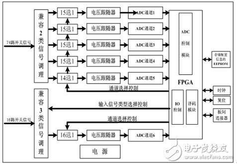
The functional block diagram of the switch signal acquisition module is shown in Figure 3.

Figure 3 Functional block diagram of the binary signal acquisition module
The FPGA of the digital signal acquisition module mainly implements the following functional modules:
2 ADC chip ADS8555SPM interface, this interface requires buffer space, used to cache the ADC acquisition results;
2 channel selection switch MAX354 interface;
2 16-channel GPIO (resistance selection for controlling the input range of the acquisition channel);
2 channel configuration information memory EEPROM AT24C16A control interface;
2 1 channel FPGA own heartbeat pulse output;
2 various filtering algorithms for switching signal acquisition;
The FPGA power-on workflow is: Power-on->Read Channel Configuration Information Memory EEPROM->Set the channel hardware according to the configuration information (whether the channel is enabled, the channel input range (depending on the range determines whether the channel has a pull-up resistor)) - "Start polling the acquisition results of one channel every 0.1 μs and buffering it -" Waiting for S698T to read the cached data;
The functional block diagram of the analog signal acquisition module is shown in Figure 4.

Figure 4 Functional block diagram of the analog signal acquisition module
The FPGA of the analog signal acquisition module mainly implements the following functional modules:
2 ADC chip ADS8555SPM interface, this interface requires buffer space, used to cache the ADC acquisition results;
2 channel selection switch MAX354 interface;
2 current ratio test range control switch MAX335MRG interface;
2 frequency control module, support 8 channel input (8 select 1 input);
2 channel configuration information memory EEPROM AT24C16A control interface;
2 1 channel FPGA own heartbeat pulse output;
2 filtering algorithm for analog acquisition;
Since the data acquisition of the acquisition channel is completely controlled by the FPGA (including the acquisition process), the power-on workflow of the FPGA is: Power-on->Read Channel Configuration Information Memory EEPROM->According to the configuration information (channel enable, channel input) Range) Set the hardware of the channel - "Start polling the acquisition results of one channel every 0.1 μs and buffer it up -" Wait for S698T to read the cached data;
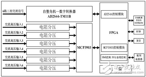
The block diagram of the AC signal acquisition module is shown in Figure 5. The main functions are as follows:

Figure 5 Functional block diagram of the AC signal acquisition module
2 self-aligning machine - data converter chip AD2S44 interface, this interface requires buffer space, used to cache the ADC acquisition results;
2 AC signal acquisition chip MCP3903 interface;
2 channel configuration information memory EEPROM AT24C16A control interface;
2 1 channel FPGA own heartbeat pulse output;
2 filtering algorithm for AC signal acquisition;
The FPGA power-on workflow is initially set to: Power-on -> Read Channel Configuration Information Memory EEPROM - Set the hardware of the channel according to the configuration information (whether the channel is enabled, etc.) - Start polling the results of one channel every 0.1 μs And cache it up - "waiting for S698T to read the cached data;
3 Conclusion
The board-level debugging and experiment show that the design of the flying ginseng collector based on S698-T fully meets the needs of practical applications. At present, this type of flying ginseng collector has been widely used in actual products.
Product Name: Car Charger
Place of Origin: Guangdong, China (Mainland)
Brand Name: OEM
Output Type: DC
Connection: Other
Rated Voltage: 12V-24V
Working Temp: 0-55℃
Weight: 36g
Materials: PC+ABS
Color: White Black
Warranty: 1 year
Suitable for:Most digital devices
SMART PROTECTION & ATTRACTIVE DESIGN ------ Intelligent circuit design protects against short circuiting,over-heating,over-current,and over-charging. Charging stops when battery is full. Car charger with blue LED indicator,which makes it convenient to find exactly where the connection should go; And the light is soft enough not to distract at night.
Dual USB Car Charger Adapter,USB Smart Port Charger ,Car Charger,USB Car Charger For Phone
Shenzhen Waweis Technology Co., Ltd. , https://www.waweisasdapter.com