Abstract: Digital electronic systems enrich our lives, but digital clock signals also play a “negative roleâ€, namely conducted noise sources (via cables) or electromagnetic radiation interference (EMI). Due to potential noise problems, electronic products need to pass the test of relevant standards to ensure compliance with EMI standards. In addition to EMI compatibility, automotive electronic products also need to consider many other issues. In order to simplify the design, spread spectrum (SS) oscillators have gradually become the focus of attention in the development of automotive electronic instruments, driver and passenger assisted electronic products.
The advantages of spread-spectrum oscillators in automotive electronics design Spread-spectrum technology can well meet the requirements of FCC regulations and EMI compatibility. The quality of EMI compatibility depends largely on the passband index of the measurement technology. Spread spectrum oscillator fundamentally solves the problem of high concentration of peak energy, which is distributed in the noise floor, reducing the need for filtering and shielding of the system, while also bringing some other benefits.
High-quality multimedia, audio, video and wireless systems account for an increasing share of today's automotive electronics products, and designers have to consider the radio frequency (RF) energy distributed in the sensitive frequency bands of these subsystems. For high-quality wireless devices, whether the RF peak energy can be eliminated directly determines the effectiveness of the solution.
For many years, wireless communication products have used "frequency adjustment" technology to avoid the impact of power supply switching noise. This wireless device can communicate with the power supply, make the power supply change its switching frequency according to the instruction, and move the energy peak outside the tuner input frequency band. In modern automotive electronic products, with the increase in the number of interference sources, it is difficult to ensure the cooperative work between systems. This situation becomes more complicated due to the diversification of equipment antennas and restrictions on the placement of newly added subsystems.
Spread spectrum oscillators have unique advantages in systems such as digital audio, factory assembly, hands-free devices, etc. These systems generally use codecs to improve audio quality, and the codecs are connected to cellular phones or other information processing terminals through digital interfaces If the “jitter†(spread spectrum) oscillator is used as the clock source of the codec, harmonic noise can be eliminated under non-silent conditions. This technique is common in multimedia systems that use switched capacitor codecs. In addition to suppressing harmonic noise, the SS oscillator can reduce the energy peak to within the noise floor, which can reduce the interference falling into the channel in the wireless frequency hopping network.
In the next generation of automotive electronic products, almost all subsystems tend to use SS clock technology to improve system performance and reduce EMI. For this application, Maxim / Dallas has launched an all-silicon oscillator, which can be reliably started and has shock resistance. Its cost is extremely competitive with ceramic resonators, with oscillation frequencies ranging from a few kilohertz to tens of megahertz. The design of automotive electronic products considers that effective control of EMI is a key problem faced by electronic engineers in product design. The digital system clock is an important "source" of EMI. The main reason is that the clock generally has the highest frequency in the system, and often Periodic square wave, clock lead length is usually the longest in the system wiring. The frequency spectrum of the clock signal includes the fundamental wave and harmonics, and the amplitude of the harmonic components decreases with increasing frequency.
Other signals in the system (signals located on the data or address bus) are refreshed at a frequency synchronized with the clock, but the data refresh action occurs at uncertain time intervals and is not related to each other. The resulting noise spectrum occupies a wide frequency band, and the noise amplitude is much lower than the noise amplitude generated by the clock. Although the total noise energy generated by these signals is much higher than the clock noise energy, it has very little effect on EMI testing. EMI testing focuses on the magnitude of the highest spectral power density, not the total radiated energy.
In practical applications, EMI indicators can be improved through filtering, shielding, and good PC board layout. However, adding filters and shielding will increase the cost of the system, and precise circuit board layout takes a long time. Another way to solve the EMI problem is to start directly from the noise source (usually a clock oscillator), generating a clock frequency that changes with time can easily reduce the fundamental and harmonic amplitudes.
The energy of the clock signal is constant. A clock with a changing frequency broadens the frequency spectrum and thus reduces the energy of each harmonic component. A simple method of generating such a clock is to modulate a voltage controlled oscillator (VCO) with a triangular wave, and the resulting clock spectrum range increases as the amplitude of the triangular wave increases. In practical applications, it is necessary to reasonably select the repetition period of the triangle wave. When the triangle wave frequency is low, coupling noise will be generated to the analog subsystem through the power supply; if the triangle wave is selected to be too high, it will interfere with the digital circuit.
Figure 1 is a schematic diagram of a clock oscillator based on the above considerations. It uses a triangular wave to control the bandwidth of the VCO output spectrum. The center frequency of the VCO is controlled by a DAC and a programmable 8-bit divider. The frequency can be set in the range of 260kHz to 133MHz. The IC shown in Figure 1 is controlled through a 2-wire interface, and the control word is stored in the EEPROM inside the chip. If the frequency is set at the desired frequency point in advance, the device can work in stand-alone mode or update the frequency during its idle period , Which is also an advantage in low-power applications.
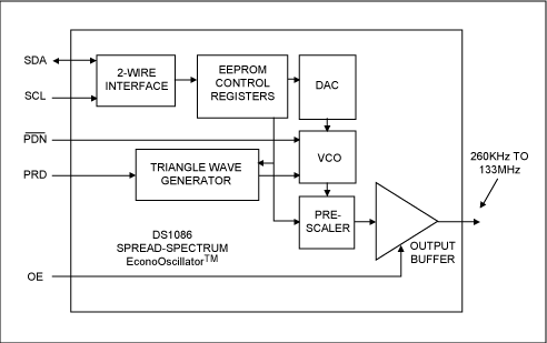
Figure 1 The core circuit of the DS1086 programmable clock generator is a VCO controlled by a triangle wave. The frequency is programmed through a 2-wire interface and stored in the on-chip EEPROM.
Figure 2 shows a comparison chart of the frequency spectrum of an ordinary crystal oscillator and a spread-spectrum clock oscillator. By setting the amplitude of the triangle wave, the spectrum can be expanded by 4%, and the peak amplitude is reduced by nearly 25dB compared with the crystal clock oscillator.
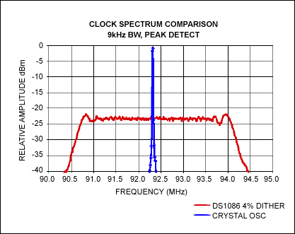
Figure 2. The spectrum of the crystal oscillator is compared with the DS1086 spectrum. The difference is 25dB when the spectrum is spread by 4%.
When using the spread spectrum oscillator as the clock source of the microprocessor, it must be confirmed that the microprocessor can accept the clock duty control ratio, rise / fall time and other parameter tolerances caused by the change of the clock source frequency. When the oscillator is used as the system's reference clock (real-time clock or real-time monitoring, etc.), frequency changes may cause large errors.
Many portable consumer products have radio frequency functions, such as cellular phones, and spread-spectrum technology is very beneficial for switching power supplies in such products. Radio frequency circuits (especially VCO) are very sensitive to power supply noise, but portable products must use switching power supplies in order to extend the life of the battery to provide efficient voltage conversion. The switching power supply has the same noise spectrum as the clock oscillator, and the noise can be directly coupled to the RF circuit, which affects the performance of the system.
A boost converter with external synchronization (such as the MAX1703) can use a spread-spectrum clock to control its oscillation frequency. This scheme can improve system performance compared to the noise spectrum of a self-oscillation boost converter (Figure 3) ( Figure 4). The harmonics of the self-oscillation boost converter have greater energy in the entire 10MHz range, while the spread-spectrum scheme reduces the amplitude of the harmonic components to within the noise floor (Figure 4). It is worth noting that since the total noise energy is fixed, the noise floor is increased after spreading.
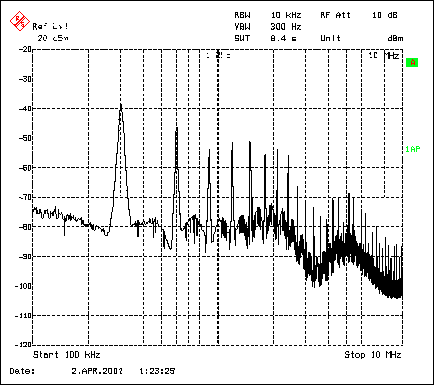
Figure 3. The MAX1703 boost converter spectrum shows that the fundamental wave is at 300kHz (self-oscillation switching frequency), and there are significant harmonics in the entire frequency band up to 10MHz.
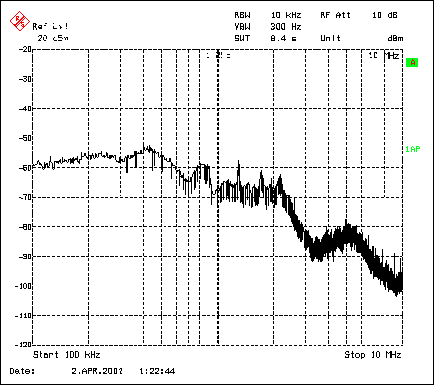
Figure 4. Synchronizing the MAX1703 boost converter to a spread spectrum can eliminate the spiked spectrum and increase the overall noise floor.
Before adding jitter to the clock source, you need to consider the following questions: What kind of "jitter" waveform needs to be used? What is the maximum clock skew allowed? What jitter rate is required? What are the factors that limit the jitter rate? The following discusses these issues. In order to ensure that the clock signal can be accepted by the system, the “jitter†waveform is generally smaller (<10%). In this way, the "jitter" process is very similar to narrow-band FM modulation.
The corresponding modulation theory gives a simple relationship between the jitter waveform and the spectrum result, that is: the "probability density function" of the clock frequency has the same shape as the frequency spectrum of the jitter clock output, and the sawtooth wave is a common "jitter" Waveform, each dithering cycle can accurately enter each frequency twice. Since each frequency point has the same proportion of time, the probability density function maintains a constant with the change of frequency in the entire frequency adjustment range, and a uniform probability distribution is obtained (Figure 1).
The frequency spectrum of this jitter waveform is the same, and the spectrum energy is evenly distributed in a narrow frequency band. For the allowed (Fmax-Fmin) frequency range, this spectrum distribution is the best because it is at each frequency point The resulting spectral energy is the lowest.
This frequency spectrum can also be obtained using a pseudo-random frequency jitter. This method usually generates a long sequence of frequencies and repeats them at a certain interval. Each frequency point appears only once in a cycle, and the resulting probability density distribution is also Uniform, the same as the triangular ditherer. This method is usually used in other fields. Spectrum attenuation examines the quality of a jitter clock circuit, mainly to see how much the energy of each frequency point in the narrow-band spectrum is reduced relative to the energy of the single-tone clock. This section derives a relationship for optimizing the uniform spread spectrum waveform.
The following points are helpful in understanding the energy of the spread spectrum: 1. The conversion from a single tone to a jitter clock does not change the clock energy, but the energy of the single tone clock after dithering is distributed in a wider frequency band. 2. The frequency spectrum of the periodic "jitter" clock consists of harmonics at intervals of the "jitter" frequency (Fd). The following formula divides the tone power evenly into the entire jitter harmonic band:
VRMS (dB) = 20log [sqrt ({(F0 * a) / Fd} * Vu2)]
= 10log [{(F0 * a) / Fd}] + 20log [Vu],
In the formula: F0 is the frequency before adding jitter, a is the jitter coefficient relative to the non-jitter frequency, and Vu is the RMS voltage of each spectrum in the jitter clock band. Therefore, the attenuation of the spectrum energy in the narrow-band frequency band can be obtained as:
Spectrum attenuation = 10log [{(F0 * a) / Fd}].
The above equation shows that the more harmonics of the spectrum generated within the allowed jitter clock bandwidth (a * F0), the lower the energy of the spectrum. As an example, we can examine the jitter structure of the DS1086 programmable clock generator. In the DS1086 circuit, a = 0.04, F0 = 100MHz, and Fd = F0 / 2048. Therefore, the spectrum attenuation of the DS1086 is 19.1dB.
Note that increasing the jitter coefficient (a) can achieve the same purpose as reducing the "jitter" rate. In addition, this equation applies to both triangular wave jitter and pseudo-random jitter because they have the same distribution. Jitter limitation Some factors in practical applications will limit the amount of attenuation of spectrum energy. First, because jitter changes the system timing, there is frequency instability. According to this, the system defines a limit for parameter "a".
The circuit that generates the jitter clock will also limit the rate of "jitter". In systems with a phase-locked loop or other control loop (such as DS1086), the "jitter" control voltage is limited by the bandwidth of the control loop. Otherwise, the distribution function of jitter control will be transformed into a Gaussian function, and the resulting spectrum energy will be mainly concentrated around the non-jitter clock frequency.
The main frequency of the triangular wave jitter clock structure is at its jitter rate, while the pseudo-random jitter clock structure requires the frequency band to be higher than the rate of the jitter template. The frequency can jump from the minimum value to the maximum value, and the frequency in the triangular wave template is continuously increasing. The following approximate relationship between loop bandwidth and jitter rate:
Loop bandwidth> 3 (triangle template rate)
Loop bandwidth> 3 (Pseudo-random template rate)
When the loop bandwidth is fixed, the triangular wave template can support a higher jitter frequency. Because the jitter rate must be faster than the narrowband detection of interference (in the form of frequency jitter), for the same detection time, the jitter rate of the triangular wave template is higher than that of the pseudo-random template.
The jitter detection time directly affects the minimum jitter rate, the frequency band of the interfering signal depends on the specific application, and there is no certain lower limit for the jitter frequency. Another consideration for the lower limit of the jitter frequency is the out-of-band noise generated by the jitter rate itself. For linear systems, the triangular wave dither does not generate harmonics at the dither rate. However, if the non-linear circuit picks up the clock signal, some undesirable spectrum components will be generated, and the low jitter frequency will be mixed to produce an interference signal in the effective operating frequency band.
Spread spectrum technology is not used to replace the traditional EMI suppression technology, such as: filtering, shielding and good circuit board layout. This technology can fundamentally improve the performance of the system, especially for devices where subsystems or peripherals are susceptible to peak energy interference. It can greatly reduce radio frequency / TV interference in automobile products or home entertainment equipment. Good PCB layout is the basic guarantee for the normal operation of the system. Spread spectrum clocks help the system to pass EMI certification, and can reduce the system's need for filtering and shielding, and reduce system costs.
For Samsung:
For Galaxy S6, For Galaxy S6 Edge, For Galaxy S6 Edge+,
For Galaxy S6 Active, For Galaxy S6 Duos, For Galaxy Note Edge,
For Galaxy S7, For Galaxy S7 Edge, For Galaxy Note 5
For Galaxy S8, For Galaxy S8 Plus, For Galaxy Note 8
For Galaxy S9,For Galaxy S9 Plus
For Sony:
For Xperia Z4V, For Xperia Z3V
For Google:
For Nexus 4, For Nexus 5, For Nexus 6, For Nexus 7
For MOTORALA:
For Moto Droid Turbo, For Moto Droid Turbo 2, For Moto Droid 5
For NOKIA:
For Lumia 920, For Lumia 928, For Nokia Lumia 93, For Lumia 950, For Lumia 950 XL, For Lumia 1020, For Nokia Lumia 1050, For Nokia Lumia 822, For Nokia Lumia 735
For HTC:
For HTC ONE MAX T6, For HTC Incredible 4G, For HTC ONE mini 2, For HTC Droid DNA
For LG:
For LG Nexus 4, For LG Nexus 5, For LG G Pro, For LG D1L, For LG LTE2
For Others:
For YotaPhone 2, For Elephone P9000
High-quality multimedia, audio, video and wireless systems account for an increasing share of today's automotive electronics products, and designers have to consider the radio frequency (RF) energy distributed in the sensitive frequency bands of these subsystems. For high-quality wireless devices, whether the RF peak energy can be eliminated directly determines the effectiveness of the solution.
For many years, wireless communication products have used "frequency adjustment" technology to avoid the impact of power supply switching noise. This wireless device can communicate with the power supply, make the power supply change its switching frequency according to the instruction, and move the energy peak outside the tuner input frequency band. In modern automotive electronic products, with the increase in the number of interference sources, it is difficult to ensure the cooperative work between systems. This situation becomes more complicated due to the diversification of equipment antennas and restrictions on the placement of newly added subsystems.
Spread spectrum oscillators have unique advantages in systems such as digital audio, factory assembly, hands-free devices, etc. These systems generally use codecs to improve audio quality, and the codecs are connected to cellular phones or other information processing terminals through digital interfaces If the “jitter†(spread spectrum) oscillator is used as the clock source of the codec, harmonic noise can be eliminated under non-silent conditions. This technique is common in multimedia systems that use switched capacitor codecs. In addition to suppressing harmonic noise, the SS oscillator can reduce the energy peak to within the noise floor, which can reduce the interference falling into the channel in the wireless frequency hopping network.
In the next generation of automotive electronic products, almost all subsystems tend to use SS clock technology to improve system performance and reduce EMI. For this application, Maxim / Dallas has launched an all-silicon oscillator, which can be reliably started and has shock resistance. Its cost is extremely competitive with ceramic resonators, with oscillation frequencies ranging from a few kilohertz to tens of megahertz. The design of automotive electronic products considers that effective control of EMI is a key problem faced by electronic engineers in product design. The digital system clock is an important "source" of EMI. The main reason is that the clock generally has the highest frequency in the system, and often Periodic square wave, clock lead length is usually the longest in the system wiring. The frequency spectrum of the clock signal includes the fundamental wave and harmonics, and the amplitude of the harmonic components decreases with increasing frequency.
Other signals in the system (signals located on the data or address bus) are refreshed at a frequency synchronized with the clock, but the data refresh action occurs at uncertain time intervals and is not related to each other. The resulting noise spectrum occupies a wide frequency band, and the noise amplitude is much lower than the noise amplitude generated by the clock. Although the total noise energy generated by these signals is much higher than the clock noise energy, it has very little effect on EMI testing. EMI testing focuses on the magnitude of the highest spectral power density, not the total radiated energy.
In practical applications, EMI indicators can be improved through filtering, shielding, and good PC board layout. However, adding filters and shielding will increase the cost of the system, and precise circuit board layout takes a long time. Another way to solve the EMI problem is to start directly from the noise source (usually a clock oscillator), generating a clock frequency that changes with time can easily reduce the fundamental and harmonic amplitudes.
The energy of the clock signal is constant. A clock with a changing frequency broadens the frequency spectrum and thus reduces the energy of each harmonic component. A simple method of generating such a clock is to modulate a voltage controlled oscillator (VCO) with a triangular wave, and the resulting clock spectrum range increases as the amplitude of the triangular wave increases. In practical applications, it is necessary to reasonably select the repetition period of the triangle wave. When the triangle wave frequency is low, coupling noise will be generated to the analog subsystem through the power supply; if the triangle wave is selected to be too high, it will interfere with the digital circuit.
Figure 1 is a schematic diagram of a clock oscillator based on the above considerations. It uses a triangular wave to control the bandwidth of the VCO output spectrum. The center frequency of the VCO is controlled by a DAC and a programmable 8-bit divider. The frequency can be set in the range of 260kHz to 133MHz. The IC shown in Figure 1 is controlled through a 2-wire interface, and the control word is stored in the EEPROM inside the chip. If the frequency is set at the desired frequency point in advance, the device can work in stand-alone mode or update the frequency during its idle period , Which is also an advantage in low-power applications.
Figure 1 The core circuit of the DS1086 programmable clock generator is a VCO controlled by a triangle wave. The frequency is programmed through a 2-wire interface and stored in the on-chip EEPROM.
Figure 2 shows a comparison chart of the frequency spectrum of an ordinary crystal oscillator and a spread-spectrum clock oscillator. By setting the amplitude of the triangle wave, the spectrum can be expanded by 4%, and the peak amplitude is reduced by nearly 25dB compared with the crystal clock oscillator.
Figure 2. The spectrum of the crystal oscillator is compared with the DS1086 spectrum. The difference is 25dB when the spectrum is spread by 4%.
When using the spread spectrum oscillator as the clock source of the microprocessor, it must be confirmed that the microprocessor can accept the clock duty control ratio, rise / fall time and other parameter tolerances caused by the change of the clock source frequency. When the oscillator is used as the system's reference clock (real-time clock or real-time monitoring, etc.), frequency changes may cause large errors.
Many portable consumer products have radio frequency functions, such as cellular phones, and spread-spectrum technology is very beneficial for switching power supplies in such products. Radio frequency circuits (especially VCO) are very sensitive to power supply noise, but portable products must use switching power supplies in order to extend the life of the battery to provide efficient voltage conversion. The switching power supply has the same noise spectrum as the clock oscillator, and the noise can be directly coupled to the RF circuit, which affects the performance of the system.
A boost converter with external synchronization (such as the MAX1703) can use a spread-spectrum clock to control its oscillation frequency. This scheme can improve system performance compared to the noise spectrum of a self-oscillation boost converter (Figure 3) ( Figure 4). The harmonics of the self-oscillation boost converter have greater energy in the entire 10MHz range, while the spread-spectrum scheme reduces the amplitude of the harmonic components to within the noise floor (Figure 4). It is worth noting that since the total noise energy is fixed, the noise floor is increased after spreading.
Figure 3. The MAX1703 boost converter spectrum shows that the fundamental wave is at 300kHz (self-oscillation switching frequency), and there are significant harmonics in the entire frequency band up to 10MHz.
Figure 4. Synchronizing the MAX1703 boost converter to a spread spectrum can eliminate the spiked spectrum and increase the overall noise floor.
Before adding jitter to the clock source, you need to consider the following questions: What kind of "jitter" waveform needs to be used? What is the maximum clock skew allowed? What jitter rate is required? What are the factors that limit the jitter rate? The following discusses these issues. In order to ensure that the clock signal can be accepted by the system, the “jitter†waveform is generally smaller (<10%). In this way, the "jitter" process is very similar to narrow-band FM modulation.
The corresponding modulation theory gives a simple relationship between the jitter waveform and the spectrum result, that is: the "probability density function" of the clock frequency has the same shape as the frequency spectrum of the jitter clock output, and the sawtooth wave is a common "jitter" Waveform, each dithering cycle can accurately enter each frequency twice. Since each frequency point has the same proportion of time, the probability density function maintains a constant with the change of frequency in the entire frequency adjustment range, and a uniform probability distribution is obtained (Figure 1).
The frequency spectrum of this jitter waveform is the same, and the spectrum energy is evenly distributed in a narrow frequency band. For the allowed (Fmax-Fmin) frequency range, this spectrum distribution is the best because it is at each frequency point The resulting spectral energy is the lowest.
This frequency spectrum can also be obtained using a pseudo-random frequency jitter. This method usually generates a long sequence of frequencies and repeats them at a certain interval. Each frequency point appears only once in a cycle, and the resulting probability density distribution is also Uniform, the same as the triangular ditherer. This method is usually used in other fields. Spectrum attenuation examines the quality of a jitter clock circuit, mainly to see how much the energy of each frequency point in the narrow-band spectrum is reduced relative to the energy of the single-tone clock. This section derives a relationship for optimizing the uniform spread spectrum waveform.
The following points are helpful in understanding the energy of the spread spectrum: 1. The conversion from a single tone to a jitter clock does not change the clock energy, but the energy of the single tone clock after dithering is distributed in a wider frequency band. 2. The frequency spectrum of the periodic "jitter" clock consists of harmonics at intervals of the "jitter" frequency (Fd). The following formula divides the tone power evenly into the entire jitter harmonic band:
VRMS (dB) = 20log [sqrt ({(F0 * a) / Fd} * Vu2)]
= 10log [{(F0 * a) / Fd}] + 20log [Vu],
In the formula: F0 is the frequency before adding jitter, a is the jitter coefficient relative to the non-jitter frequency, and Vu is the RMS voltage of each spectrum in the jitter clock band. Therefore, the attenuation of the spectrum energy in the narrow-band frequency band can be obtained as:
Spectrum attenuation = 10log [{(F0 * a) / Fd}].
The above equation shows that the more harmonics of the spectrum generated within the allowed jitter clock bandwidth (a * F0), the lower the energy of the spectrum. As an example, we can examine the jitter structure of the DS1086 programmable clock generator. In the DS1086 circuit, a = 0.04, F0 = 100MHz, and Fd = F0 / 2048. Therefore, the spectrum attenuation of the DS1086 is 19.1dB.
Note that increasing the jitter coefficient (a) can achieve the same purpose as reducing the "jitter" rate. In addition, this equation applies to both triangular wave jitter and pseudo-random jitter because they have the same distribution. Jitter limitation Some factors in practical applications will limit the amount of attenuation of spectrum energy. First, because jitter changes the system timing, there is frequency instability. According to this, the system defines a limit for parameter "a".
The circuit that generates the jitter clock will also limit the rate of "jitter". In systems with a phase-locked loop or other control loop (such as DS1086), the "jitter" control voltage is limited by the bandwidth of the control loop. Otherwise, the distribution function of jitter control will be transformed into a Gaussian function, and the resulting spectrum energy will be mainly concentrated around the non-jitter clock frequency.
The main frequency of the triangular wave jitter clock structure is at its jitter rate, while the pseudo-random jitter clock structure requires the frequency band to be higher than the rate of the jitter template. The frequency can jump from the minimum value to the maximum value, and the frequency in the triangular wave template is continuously increasing. The following approximate relationship between loop bandwidth and jitter rate:
Loop bandwidth> 3 (triangle template rate)
Loop bandwidth> 3 (Pseudo-random template rate)
When the loop bandwidth is fixed, the triangular wave template can support a higher jitter frequency. Because the jitter rate must be faster than the narrowband detection of interference (in the form of frequency jitter), for the same detection time, the jitter rate of the triangular wave template is higher than that of the pseudo-random template.
The jitter detection time directly affects the minimum jitter rate, the frequency band of the interfering signal depends on the specific application, and there is no certain lower limit for the jitter frequency. Another consideration for the lower limit of the jitter frequency is the out-of-band noise generated by the jitter rate itself. For linear systems, the triangular wave dither does not generate harmonics at the dither rate. However, if the non-linear circuit picks up the clock signal, some undesirable spectrum components will be generated, and the low jitter frequency will be mixed to produce an interference signal in the effective operating frequency band.
Spread spectrum technology is not used to replace the traditional EMI suppression technology, such as: filtering, shielding and good circuit board layout. This technology can fundamentally improve the performance of the system, especially for devices where subsystems or peripherals are susceptible to peak energy interference. It can greatly reduce radio frequency / TV interference in automobile products or home entertainment equipment. Good PCB layout is the basic guarantee for the normal operation of the system. Spread spectrum clocks help the system to pass EMI certification, and can reduce the system's need for filtering and shielding, and reduce system costs.
For Iphone:
For Iphone8/X/XR/XS Max
Compabile Models:
For Samsung:
For Galaxy S6, For Galaxy S6 Edge, For Galaxy S6 Edge+,
For Galaxy S6 Active, For Galaxy S6 Duos, For Galaxy Note Edge,
For Galaxy S7, For Galaxy S7 Edge, For Galaxy Note 5
For Galaxy S8, For Galaxy S8 Plus, For Galaxy Note 8
For Galaxy S9,For Galaxy S9 Plus
For Sony:
For Xperia Z4V, For Xperia Z3V
For Google:
For Nexus 4, For Nexus 5, For Nexus 6, For Nexus 7
For MOTORALA:
For Moto Droid Turbo, For Moto Droid Turbo 2, For Moto Droid 5
For NOKIA:
For Lumia 920, For Lumia 928, For Nokia Lumia 93, For Lumia 950, For Lumia 950 XL, For Lumia 1020, For Nokia Lumia 1050, For Nokia Lumia 822, For Nokia Lumia 735
For HTC:
For HTC ONE MAX T6, For HTC Incredible 4G, For HTC ONE mini 2, For HTC Droid DNA
For LG:
For LG Nexus 4, For LG Nexus 5, For LG G Pro, For LG D1L, For LG LTE2
For Others:
For YotaPhone 2, For Elephone P9000
Guangzhou HangDeng Tech Co. Ltd , https://www.hangdengtech.com