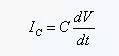
First, PCB traces in the middle of capacitive load reflection Many times, PCB traces will pass through the hole, test point pad, short stub line, etc., there are parasitic capacitance, which will inevitably affect the signal. The effect of the capacitance in the middle of the line on the signal should be analyzed from both the transmitting end and the receiving end, affecting both the starting point and the ending point. First click to see the effect on the signal transmitter. When a fast rising step signal reaches the capacitor, the capacitor is quickly charged, and the charging current is related to the rising speed of the signal voltage. The charging current formula is: I=C*dV/dt. The larger the capacitance, the larger the charging current, the faster the signal rise time, and the smaller the dt, the larger the charging current.
We know that the reflection of the signal is related to the impedance change experienced by the signal, so for analysis, let's look at the impedance change caused by the capacitance. At the beginning of the capacitor charging, the impedance is expressed as: 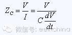
Here dV is actually the step signal voltage change, dt is the signal rise time, and the capacitance impedance formula becomes: 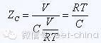
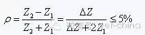
From this formula, we can get a very important information. When the step signal is applied to the two ends of the capacitor, the impedance of the capacitor is related to the rise time of the signal and its own capacitance. Usually at the beginning of capacitor charging, the impedance is small and less than the characteristic impedance of the trace. The signal is negatively reflected at the capacitor. This negative voltage signal is superimposed with the original signal, causing the signal at the transmitting end to undershoot, causing the non-monotonicity of the signal at the transmitting end. For the receiving end, after the signal reaches the receiving end, a positive reflection occurs, and the reflected signal reaches the position of the capacitor. That kind of negative reflection occurs, and the negative reflection voltage reflected back to the receiving end also causes the receiving end signal to undershoot. In order for the reflected noise to be less than 5% of the voltage swing (which can be tolerated by the signal), the impedance change must be less than 10%. So what is the capacitance impedance should be controlled? The impedance of the capacitor appears as a parallel impedance, and we can use the parallel impedance equation and the reflection coefficient formula to determine its range. For this parallel impedance, we hope that the larger the capacitor impedance, the better. Assuming that the capacitive impedance is k times the characteristic impedance of the PCB trace, the impedance experienced by the signal at the capacitor according to the parallel impedance equation is: 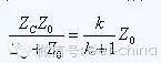
The rate of change of impedance is:
 , which is
  That is, according to this ideal calculation, the impedance of the capacitor must be at least 9 times the characteristic impedance of the PCB. In fact, as the capacitor is charged, the impedance of the capacitor increases, not always maintaining the lowest impedance. In addition, each device also has parasitic inductance, which increases the impedance. So this 9-fold limit can be relaxed. In the discussion below, this limit is assumed to be five times. With the impedance indicator, we can determine how much capacitance can be tolerated. The 50 ohm characteristic impedance on the board is very common, I use 50 ohms to calculate.
 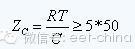 inferred:
 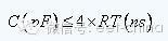 That is, in this case, if the signal rise time is 1 ns, the capacitance is less than 4 picofarads. Conversely, if the capacitance is 4 picofarads, the signal rise time is as fast as 1 ns. If the signal rise time is 0.5 ns, this 4 picofarad capacitor will cause problems. The calculation here is only to explain the influence of the capacitor. The actual circuit is very complicated and there are more factors to consider. Therefore, the accuracy of the calculation here has no practical significance. The key is to understand how the capacitance affects the signal through this calculation. Once we have a perceptual understanding of the impact of each of the factors on the board, we can provide the necessary guidance for the design, and know how to analyze it when problems arise. Accurate evaluation requires software to simulate. Summary: 1 The capacitive load in the middle of the PCB trace causes the signal at the transmitter to undershoot, and the signal at the receiver also generates an undershoot. 2 The capacity that can be tolerated is related to the rise time of the signal. The faster the signal rises, the smaller the capacity that can be tolerated. Second, the receiving end of the reflected signal of the receiving end capacitive load may be a pin of the integrated chip, or other components. Regardless of the receiving end, the actual device input must have parasitic capacitance, the chip pin receiving the signal and the adjacent pin have a certain parasitic capacitance, and the internal wiring of the chip connected to the pin also has parasitic capacitance. There is also a parasitic capacitance between the pin and the signal return path. So complicated, so many parasitic capacitors! In fact, it is very simple, think about what is the capacitor? Two metal plates with an insulating medium in between. This definition does not say what the shape of the two metal plates is. The two adjacent pins of the chip can also be regarded as two metal plates of the capacitor. The intermediate medium is air, not a capacitor. The power supply or ground plane of the chip pins and the inner layer of the PCB is also a pair of metal plates. The intermediate medium is the board of the PCB board. The common one is the FR4 material, which is also a capacitor. Oh, let's get it done, or go back to the most basic part. Masters don't laugh, it's too simple. However, many people feel a little dizzy when they see the parasitic capacitance. They don't understand it, so let's take a look here. Going back to the topic, let's examine what effect the capacitance of the signal terminal has. Simplify the model and replace all parasitic capacitances with a discrete capacitive component, as shown in Figure 1.
We examine the impedance of the capacitor at point B. The current of the capacitor is:
As the capacitor is charged, the voltage change rate is gradually reduced (transient process in the circuit principle), and the charging current of the capacitor is also continuously reduced. That is, the charging current of the capacitor changes with time.
The impedance of the capacitor is:
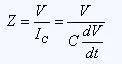
Therefore, the impedance exhibited by the capacitor changes with time and is not constant. It is this change in impedance that determines the specificity of the effect of the capacitor on the signal. If the signal rise time is less than the charging time of the capacitor, the voltage across the capacitor initially rises rapidly and the impedance is small. As the capacitor is charged, the rate of voltage change decreases, and the charging current decreases, which is manifested by a significant increase in impedance. When the charging time is infinite, the capacitance is equivalent to an open circuit and the impedance is infinite.
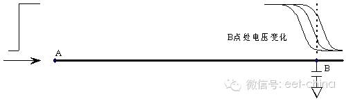
Changes in impedance necessarily affect the reflection of the signal. At the beginning of charging, the impedance is small, less than the characteristic impedance of the transmission line, negative reflection will occur, and the signal reflected back to the source A will generate an undershoot. As the impedance of the capacitor increases, the reflection gradually transitions to positive reflection, and the signal at point A gradually rises after an undershoot, eventually reaching the open circuit voltage. Therefore, the capacitive load causes a local voltage dip in the source signal. The exact waveform is related to the characteristic impedance, capacitance, and signal rise time of the transmission line. For the receiver, it is obvious that it is an RC charging circuit, not very rigorous, but very similar to the actual situation. The voltage across the capacitor, point B, increases exponentially with the time constant of the RC charging circuit (basic circuit principle). Therefore, the capacitance has an influence on the rise time of the signal at the receiving end. The time constant of the RC charging circuit is  This is the time required for the voltage at point B to rise to 37% of the final value of the voltage. B point voltage 10%~90% rise time is
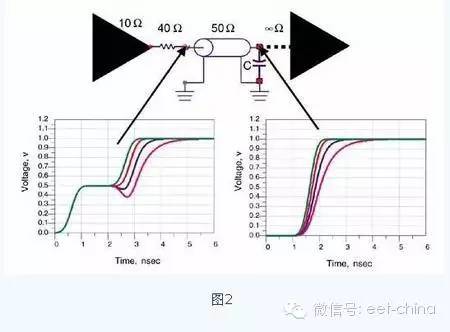
 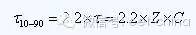 If the transmission line characteristic impedance is 50 ohms and the capacitance is 10 pF, the charging time of 10 to 90 is 1.1 ns. If the signal rise time is less than 1.1 ns, then the voltage rise time at point B is mainly determined by the capacitor charging time. If the signal rise time is greater than 1.1 ns, the end capacitor acts to extend the rise time further by about 1.1 ns (actually less than this value). Figure 2 shows a schematic diagram of the effect of the terminal capacitive load on the driver and receiver. It is here, so that everyone can have a perceptual understanding.
As for the exact value of the increase in signal rise time, it is not necessary for circuit design. As long as qualitative analysis, there is a rough estimate. Because the calculation is no more accurate, the parameters of the board are not accurate! For the designer, qualitative analysis and understanding of the impact, roughly estimate the impact at that level, can provide guidance for circuit design, and other things to do. For example, if the signal rise time is 1 ns and the capacitor increases the signal rise time by much less than 1 ns, such as 0.2 ns, then such a little increase may have no effect. If the rise time caused by the capacitor increases a lot, it may affect the circuit timing. So how much is it? Look at the timing margin of the circuit, which involves timing analysis and timing design of the circuit.
In short, there are two effects on the capacitive load at the receiving end: 1. The local (drive) signal is locally depressed. 2. The rise time of the signal at the receiving end is extended. Both points must be considered in the circuit design. Third, the reflection of the PCB trace width changes
When PCB layout is performed, it often happens that when a trace passes through an area, due to the limited wiring space of the area, thinner lines have to be used, and after passing through this area, the line is restored to its original width. A change in the width of the trace causes a change in impedance, so reflection occurs and affects the signal. So under what circumstances can this effect be ignored, and under what circumstances must we consider its impact?
Three factors are related to this effect: the magnitude of the impedance change, the rise time of the signal, and the delay of the signal on the narrow line. First, the magnitude of the impedance change will be discussed. Many circuit designs require that the reflected noise be less than 5% of the voltage swing (this is related to the noise budget on the signal), based on the reflection coefficient formula:
To calculate the approximate rate of change of the impedance is:  As you may know, the typical indicator of impedance on the board is +/-10%, the root cause is here. If the impedance change occurs only once, for example, after the line width is changed from 8 mils to 6 mils, the 6 mil width is maintained. To achieve the noise budget requirement that the signal reflection noise at the catastrophe does not exceed 5% of the voltage swing, the impedance change must be less than 10%. This is sometimes difficult to do. Take the case of the microstrip line on the FR4 board as an example. Let's calculate it. If the line width is 8 mils, the thickness between the line and the reference plane is 4 mils and the characteristic impedance is 46.5 ohms. After the line width is changed to 6 mils, the characteristic impedance becomes 54.2 ohms, and the impedance change rate reaches 20%. The amplitude of the reflected signal must exceed the standard. As for how much impact on the signal, it is also related to the signal rise time and the delay of the signal from the drive end to the reflection point. But at least this is a potential problem. Fortunately, the problem can be solved by impedance matching termination. If the impedance change occurs twice, for example, after the line width is changed from 8 mils to 6 mils, it is pulled back 2 cm and then changed back to 8 mils. Then, reflection occurs at both end points of a 2cm long 6mil wide line. Once the impedance is increased, positive reflection occurs, and then the impedance becomes small and negative reflection occurs. If the two reflection intervals are short enough, the two reflections may cancel each other out, thus reducing the effect. Assuming that the transmitted signal is 1V, the first positive reflection has 0.2V reflected, 1.2V continues to transmit forward, and the second reflection has -0.2*1.2 = 0.24v reflected back. Assuming that the length of the 6mil line is extremely short and the two reflections occur almost simultaneously, the total reflected voltage is only 0.04V, which is less than 5% of the noise budget requirement. Therefore, whether or not this reflection affects the signal has a large influence on the delay at the impedance change and the rise time of the signal. Research and experiments have shown that as long as the delay at the impedance change is less than 20% of the signal rise time, the reflected signal will not cause problems. If the signal rise time is 1 ns, then the delay at the impedance change is less than 0.2 ns for 1.2 inches, and reflection does not cause problems. That is to say, for the case of this example, the length of the 6 mil wide trace is less than 3 cm and there is no problem. When the PCB trace width changes, it should be carefully analyzed according to the actual situation, whether it will affect. The parameters to be concerned are three: how big is the impedance change, what is the signal rise time, and how long the neck portion of the line width changes. According to the above method, it is estimated roughly, and a certain margin is appropriately reserved. If possible, try to reduce the length of the neck. It should be pointed out that in actual PCB processing, the parameters cannot be as accurate as in theory. The theory can provide guidance for our design, but it cannot be copied and cannot be dogmatic. After all, this is a practical science. The estimated value should be appropriately revised according to the actual situation and applied to the design. If you feel that you are not experienced enough, then you should first keep it conservative and then adjust it according to the manufacturing cost. 4. The reflection of the signal ringing may cause ringing. A typical signal ringing is shown in Figure 1.
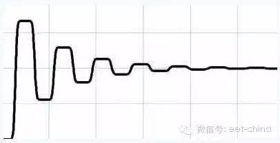
figure 1
So how does the signal ringing come about? As mentioned earlier, if the impedance changes during the signal transmission, the reflection of the signal will occur. This signal may be the signal from the driver or the reflected signal from the far end. According to the formula of the reflection coefficient, when the signal senses that the impedance becomes small, negative reflection occurs, and the reflected negative voltage causes the signal to undershoot. The signal is reflected multiple times between the driver and the far end load, and the result is a signal ringing. Most chips have low output impedance. If the output impedance is less than the characteristic impedance of the PCB trace, then signal ringing will occur if there is no source termination. The process of signal ringing can be explained intuitively using a bounce map. Assume that the output impedance of the driver is 10 ohms, and the characteristic impedance of the PCB trace is 50 ohms (can be adjusted by changing the PCB trace width, the dielectric trace between the PCB trace and the inner reference plane). For the convenience of analysis, it is assumed that the open end is open. That is, the far end impedance is infinite. The driver transmits a 3.3V voltage signal. We followed the signal to run once in this transmission line to see what happened? For the convenience of analysis, the effects of parasitic capacitance and parasitic inductance of the transmission line are ignored, and only the resistive load is considered. Figure 2 is a schematic view of the reflection. The first reflection: the signal is emitted from the inside of the chip. After 10 ohms output impedance and 50 ohm PCB characteristic impedance, the signal actually applied to the PCB trace is A point voltage 3.3*50/(10+50)=2.75 V. Transmission to the remote B point, because the B point is open, the impedance is infinite, the reflection coefficient is 1, that is, the signal is totally reflected, and the reflected signal is also 2.75V. At this time, the measurement voltage at point B is 2.75 + 2.75 = 5.5V. The second reflection: the reflected voltage of 2.75V returns to point A, the impedance changes from 50 ohms to 10 ohms, and negative reflection occurs. The reflected voltage at point A is -1.83V. The voltage reaches point B, and the reflection again occurs. The reflected voltage is -1.83. V. At this time, the measured voltage at point B is 5.5-1.83-1.83=1.84V. The third reflection: The voltage of -1.83V reflected back from point B reaches point A, and negative reflection occurs again, and the reflected voltage is 1.22V. When the voltage reaches point B, normal reflection occurs again, and the reflected voltage is 1.22V. At this time, the measured voltage at point B is 1.84 + 1.22 + 1.22 = 4.28V. 4th reflection: . . . . . . . . The fifth reflection: . . . . . . . . In this cycle, the reflected voltage bounces back and forth between points A and B, causing the voltage at point B to be unstable. Observe the voltage at point B: 5.5V->1.84V->4.28V->......, it can be seen that the voltage at point B will fluctuate up and down, which is the signal ringing.
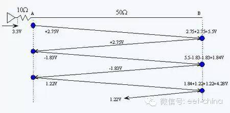
The fundamental cause of signal ringing is caused by negative reflection, and the culprit is still impedance change and impedance! When studying signal integrity issues, be sure to pay attention to impedance issues from time to time.
Ringing of the load signal can seriously interfere with signal acceptance, generate logic errors, and must be reduced or eliminated. Therefore, impedance matching termination must be performed for long transmission lines. 5. When the signal reflection signal propagates forward along the transmission line, a transient impedance is felt every moment. This impedance may be the transmission line itself, or it may be midway or other components at the end. For a signal, it doesn't distinguish exactly what it is, and the signal only senses the impedance. If the impedance felt by the signal is constant, then it will propagate forward normally, as long as the perceived impedance changes, no matter what it is caused (may be resistance, capacitance, inductance, via, PCB corner encountered in the middle) , connector), the signal will be reflected. So how much is reflected back to the starting point of the transmission line? An important measure of the amount of signal reflection is the reflection coefficient, which is the ratio of the reflected voltage to the original transmitted signal voltage. The reflection coefficient is defined as:
 among them:
  For the impedance before the change,
  For the impedance after the change. Assuming that the characteristic impedance of the PCB line is 50 ohms, a 100 ohm chip resistor is encountered during transmission. The effect of the parasitic capacitance inductance is not considered for the time being. The resistance is regarded as the ideal pure resistance, and the reflection coefficient is:
 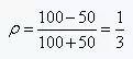 One third of the signal is reflected back to the source. If the signal is transmitted
The voltage is 3.3V and the reflected voltage is 1.1V. The reflection of a purely resistive load is the basis for studying the reflection phenomenon. The change of the resistive load is nothing more than the following four cases: the finite value of the impedance increases, the finite value decreases, the open circuit (the impedance becomes infinite), the short circuit (the impedance suddenly becomes 0) ). The finite value of the impedance increase: the above example of the reflected voltage has been calculated. At this time, there will be two voltage components at the signal reflection point, one is the 3.3V voltage from the source, and the other is the reflected voltage of 1.1V, then the voltage at the reflection point is the sum of the two, ie 4.4 V. Impedance reduction finite value: Still according to the above example, the characteristic impedance of the PCB line is 50 ohms. If the resistance encountered is 30 ohms, the reflection coefficient is 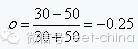 , the reflection coefficient is negative, indicating that the reflected voltage is a negative voltage, and the value is
 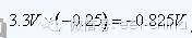 At this time, the reflection point voltage is 3.3V+(-0.825V)=2.475V. Open circuit: Open circuit is equivalent to impedance infinity, and the reflection coefficient is calculated as 1 by the formula. That is, the reflected voltage is 3.3V. The voltage at the reflection point is 6.6V. It can be seen that in this extreme case, the voltage at the reflection point is doubled. Short circuit: The impedance is 0 when short circuited and the voltage must be 0. Calculate the reflection coefficient to -1 according to the formula, indicating that the reflected voltage is -3.3V, so the reflection point voltage is zero. The calculation is very simple. It is important to know that due to the reflection phenomenon, the voltage at the point where the impedance changes in the signal propagation path is no longer the voltage originally transmitted. This reflected voltage changes the waveform of the signal and can cause signal integrity problems. This perceptual understanding is very important for studying signal integrity and designing boards, and this concept must be built up in the mind.
CCTV Microphone,Microphone For Security Camera,Cctv Audio Microphone,CCTV Audio Picker
Chinasky Electronics Co., Ltd. , https://www.cctv-products.com