Sensors are increasingly used in embedded systems. In the field of industrial products, sensors have long been used to manufacture control systems, and in the field of consumer devices, the use of sensors is on the rise. Integrating sensors into consumer products provides users with a better user experience, such as adding accelerometers to mobile phones and adding water vapor sensing to microwave ovens.
Workers who were previously only involved in digital design now find themselves having to consider the problem of connecting to an analog sensor. The analog signal of the sensor needs to be digitized before it can be used by the system. The signal path needs to go through several different stages, including amplification, filtering and digitization (see Figure 1 below). Once the signal is digitized, the user can send it to the control processing system on the microcontroller, or process the data and transmit it to the host processor via a communication protocol so that the host can use the sensor data as needed.
Each of these stages typically uses a corresponding component that should be used in conjunction with passive components to ensure proper operation of the intended application.
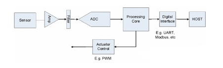
Figure 1: Sensor
sensorThe output signal and sensing distance of each sensor are different. Output signals can be based on voltage, current, resistance, capacitance or frequency, but they are only used in specific industrial systems due to the severe shortage of related standards. Even if the output of a similar sensor from the same manufacturer may be different, the above differences may cause inconvenience to the system designer. Designers must choose sensors that meet system requirements. If the system requires a change in requirements during the design process, the sensor may need to be changed accordingly. In addition, if the output of the new sensor is slightly different, it may be necessary to change the amplification and filtering stages. Since most inductors output lower current or voltage signals, this article focuses on this type of inductor. In addition, we can convert the current signal into a voltage signal through a simple resistor network. Please note: Efficiency-based considerations To improve efficiency, this article has simplified some of the concepts and device component selection processes to some extent.
The output of the sensor can be a few millivolts or a few volts. In order for the signal to be digitized correctly, the output of the sensor should be large enough to ensure that the analog-to-digital converter (ADC) reads the signal efficiently. In most cases, the sensor signal should be amplified. For example, a typical K-type thermocouple output value is 41uV/°C, which requires a full amplification of the value so that the user can get 1C accuracy. Therefore, the designer must consider the resolution of the ADC to ensure that the signal is sufficiently amplified to achieve the required granularity of accuracy.
enlargeThe choice of amplifier depends mainly on the type of amplifier required. For example, an instrumentation amplifier, a differential amplifier, an operational amplifier, or a programmable gain array is required. In addition, the amplifier needs to take into account the gain. The amplifier gain is set by a resistor network with feedback around the amplifier. The maximum gain of a standard amplifier is ideally infinite. The PGA gain is typically set by the digital signal sent to the device, which changes the internal resistor network. The maximum gain of the PGA is much more limited than traditional amplifiers, mainly between 0.5 and thousands of times, but in most cases this range of gains is sufficient.
Another important specification to consider when choosing an amplifier is the bias voltage (VOS). VOS is the voltage that the signal will change when it passes through the op amp. For example, if a 500-mV signal is input to a unity gain (1x) amplifier and the VOS is 10 mV, then the output voltage is 510 mV. If the sensor's output range is 0-900mV and the system does not require very linear reading of the sensor, the offset can be ignored. If the sensor output range is 450-550 mV, the bias can be unacceptable. When choosing an amplifier, the smaller the VOS, the higher the cost. Since all amplifiers are biased, it is important to consider whether the system can withstand this VOS. VOS can also be reduced or eliminated by correlated double sampling.
In all systems, the sensor signal is affected by noise. There are many sources of noise, such as board layout, radio, thermal noise, and even the sensor itself. Signal noise not only causes the ADC to read inaccurately and unstablely, but also increases the noise after the amplification step, thus increasing the signal error. Signal noise can be classified into low frequency, high frequency or known specific frequency noise. In most cases, what we need to solve is the high frequency noise problem.
We can filter noise in different ways, including passive analog filters, filter ICs, and digital filtering. Passive filtering is the most common method that requires the creation of passive networks that include resistors, capacitors, and inductors. The problem with passive filters is that such filters must be designed and difficult to change. As the required filter levels increase, the filter design can become more complex. The design of the first-order Chebyshev filter is much simpler than that of the eight-stage Bessel filter. Therefore, the designer first needs to specify the order level of the required filter filter before choosing which filter filtering method to use.
Filter ICs allow designers to digitally program the type of filter required. This IC creates a filter filter with built-in different types of analog circuitry and may have a bias voltage associated with itself. This IC also helps designers start the filtering process after the ADC is quantized. The design of digital filters can be very complex, but the design of high-order filters for high-level filters can be simplified with some existing tools. Digital filtering can also be an ideal way to remove noise, but this usually requires a lot of CPU resources, which in turn increases power consumption.
Digital conversionIn order to use the filtered signal of the sensor, we must quantize the analog signal to a digital value through the ADC. The choice of ADC usually takes into account the system's requirements for sample rate and resolution. The required sampling rate is related to the bandwidth of the sensor or the update frequency of the system, and the resolution depends on the finest precision required to react to the sensor information.
The mode of use of the system determines the above rate and resolution requirements. For example, a 360-degree rotation is detected with a common gyroscope, which corresponds to a voltage of 0.67 mV per degree, so that the output voltage is 241 mV. Toy helicopters may require gyroscopes with a 1 degree granularity to provide information, but 10 Ksps of throughput is required to ensure helicopter vertical. Based on the above requirements, we may need to use a 10-bit ADC, each corresponding to 0.35 ° (note that the signal is still affected by noise, on the basis of which the error is ± 1 bit is acceptable). In contrast, digital cameras that support image stabilization require 0.02-degree granularity and a low 5Ksps throughput, which allows the image sensor to be adjusted while the camera is shaking. According to the above requirements, we need to use a 16-bit ADC, each corresponding to 0.005 °.
The accuracy of the ADC is measured by integral nonlinearity (INL), differential nonlinearity (DNL), offset error, gain error, and signal-to-noise ratio (SNR). Taking all of these factors into consideration, we can understand the total error of the ADC. Figure 2 on page S10 shows each error and integrates them separately. For most applications, we don't need to consider these ADC specifications, but a serious engineer should still be aware of the specific values ​​of the ADCs used.
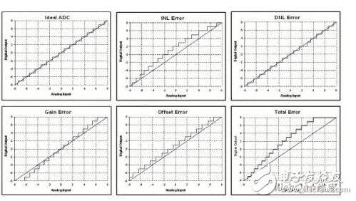
Figure 2: Combining comparison integral nonlinearity, differential nonlinearity, bias error, gain error, and signal-to-noise ratio helps us understand ADC
When selecting an ADC, the user can select an external ADC or a microcontroller with an integrated ADC. External ADCs typically perform better and perform better in terms of speed, resolution, and accuracy requirements. However, most sensor applications can be met with an integrated microcontroller ADC.
We also have a configurable ADC that includes programmable logic blocks. Integrated digital and analog programmable blocks allow us to dynamically define configurable peripherals optimized for specific sensor applications such as counters, PWMs, UARTs, SPIs, amplifiers, ADCs, and DACs. Developers can also implement signal amplification and filtering stages to integrate the entire analog signal chain in a single device (see Figure 3 above).
A configurable ADC helps to greatly simplify the design relative to passive components. In addition, developers can choose to reuse these system resources for other functions, given that the relevant module-related blocks can be dynamically reconfigured.
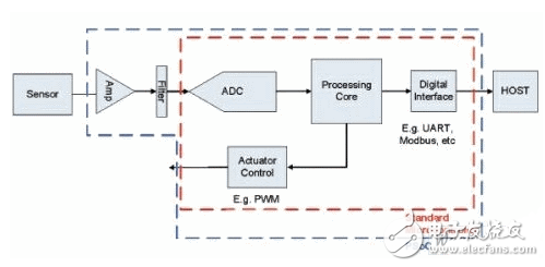
Figure 3: Developers can implement amplification and filtering stages to integrate the entire analog signal chain in a single device
Sensors continue to penetrate into a wider range of markets, giving developers more control and flexibility. Through the management of the environment (such as temperature monitoring), the sensor improves reliability, and the overall performance is improved through feedback mechanisms. In addition, various new user interfaces can be realized, and such applications are widely used. For many designs, the integrated ADC on the microcontroller provides sufficient resolution granularity and accuracy. Developers unfamiliar with analog designs may have trouble with the analog signal chain between the sensor and the MCU.
Implementing a multi-level analog signal path can be complicated, especially for people who are primarily involved in digital design work. However, by decomposing the analog signal chain into different stages of amplification, filtering, and ADC, digital developers can more easily and accurately acquire sensor data to meet the needs of a variety of industrial and consumer applications. In addition, sensor design can be greatly simplified with existing ICs, configurable ADCs, and filter filtering design tools on the market.
The small appearance and size of the One Hand Gaming Keyboard is one of the key points for users to choose.The maximum length of the keyboard in one-handed games is usually only half or even less than one third of the standard keyboard.The most comfortable position for both hands is usually slightly larger than the shoulder width of the player (the distance between the tail fingers of both hands is about 500-650mm).When using the standard keyboard, between the mouse and the keyboard. The clearance for Gaming Mouse movement is usually no more than 100mm(standard 104-key keyboard length is about 450mm). And the use of one-handed game keyboard, can let the player play with a wide mouse movement space, so that players enjoy a more rapid and flexible mouse operation.
Due to the limited size of one-handed gaming keyboards, the number of surface keys usually does not exceed the number of keys in the main key area of a standard keyboard (61 keys). Although the current PC games are designed with the first left hand key area, some secondary keys are still designed in the right hand key area for the convenience of players' memory and game operation.
For the one-handed game keyboard, comfortable ergonomic design, is to allow players to maintain long-term combat effectiveness of the basic guarantee. However, it is different from the ergonomic design of mouse in that players often move their fingers up and down and left and right when using the Gaming Keyboard.The ergonomic design that is too close to the palm will lead to the restriction of finger movement. Therefore, the ergonomic design of the one-handed game keyboard must be carried out in order to ensure that the player's finger operation is not affected.

One Hand Gaming Keyboard,Computer Gaming Keyboard,Wireless One Handed Keyboard,Single Hand Gaming Keyboard
Henan Yijiao Trading Co., Ltd , https://www.yjusbhubs.com