Since the mid-1980s, MOSFETs have been the transistor technology of choice for most switching power supplies (SMPS). The MOSFET acts as a main switching transistor and acts as a gated rectifier to increase efficiency. This design example compares P-channel and N-channel enhancement MOSFETs to select the switch that best fits the power application.
Since the mid-1980s, MOSFETs have been the transistor technology of choice for most switching power supplies (SMPS). When used as a gated rectifier, the MOSFET is the main switching transistor and combines efficiency. This design example compares P-channel and N-channel enhancement MOSFETs to select the switch that is best suited for power applications.
For marketers, MOSFETs may represent the acronym for Most Optimal Solution for Energy Transfer. For engineers, it stands for Metal Oxide Semiconductor Field Effect Transistor.
Due to the lower on-resistance (RDS(on)) and smaller size, the N-channel MOSFET exceeds the P-channel in product selection. In buck regulator applications, P-channel MOSFETs or N-channel MOSFETs are used as main switches based on various factors such as gate-controlled voltage polarity, device size, and series resistance. Synchronous rectifier applications almost always use N-channel technology, mainly because the N-channel RDS(on) is smaller than the P-channel and is turned on by applying a positive voltage across the gate.
Most of the MOSFETs are carrier devices, and the N-channel MOSFETs have electrons flowing during the conduction process. The P channel uses a positive charge called a hole during conduction. The mobility of electrons is three times that of holes. Although there is no direct correlation, in terms of RDS(on), to obtain equal values, the P-channel die size is approximately three times that of the N-channel. Therefore, the N-channel die size is smaller.
The N-channel MOSFET is turned on when a positive threshold of a suitable threshold is applied across the gate-source terminal; the P-channel MOSFET is turned on by applying a given negative gate-to-source voltage.
The gate control of the MOSFETs determines their application in SMPS converters. For example, N-channel MOSFETs are better suited for ground-referenced low-side switches, especially for boost, SEPIC, forward and isolated flyback converters. In synchronous rectifier applications and Power over Ethernet (PoE) input rectifiers, low side switches are also used instead of diodes as rectifiers. P-channel MOSFETs are most commonly used as high-side switches in buck regulators with input voltages below 15 VDC. N-channel MOSFETs can also be used as buck regulator high-side switches, depending on the application. These applications require bootstrap circuits or other forms of high side drivers.
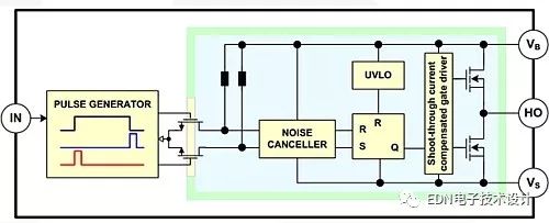
Figure 1: High side driver IC with level shifter.
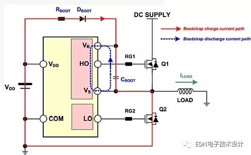
Figure 2: Gate control of the high-side N-channel MOSFET with a bootstrap circuit.
The polarity determines the graphical symbol of the MOSFET. The difference lies in the direction of the body diode and the arrow symbol with respect to the terminal.
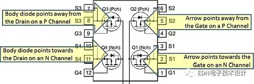
Figure 3: Schematic of a P-channel and N-channel MOSFET. Note the direction of the body diode and arrow relative to the drain (D) and source (S) terminals.
Polarity and MOSFET operating characteristics
The polarity determines the operating characteristics of the MOSFET. The positive current and voltage for the N-channel device are negative for the P-channel device.
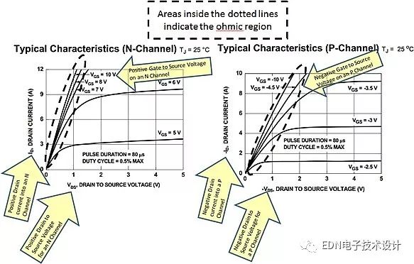
Figure 4: MOSFET first quadrant feature.
The MOSFET is "fully turned on" when there is sufficient voltage applied to the ohmic region of the gate-source terminal. In the comparison chart, the VGS of the N-channel ohmic region is 7V, and the P-channel is -4.5V.
As the gate voltage increases, the slope of the ohmic curve becomes steeper, indicating that the device is more conductive. The higher the applied gate voltage, the smaller the RDS(on) of the MOSFET. In some applications, gated MOSFETs are voltages that provide a satisfactory RDS(on). The extra gate voltage generates power due to 1â„2C x Vgs x Vgs xf, where gate charge and switching frequency play an important role in determining the ultimate operating point and choice of MOSFET technology.
The MOSFET can operate in either the first quadrant or the third quadrant. When the gate-source voltage is not applied, the parasitic body diode is turned on. When there is no voltage at the gate, the current flowing into the drain is similar to a typical diode curve.

Figure 5: Typical characteristics of an un-gated N-channel MOSFET operating in the third quadrant.
When the gate voltage is applied, a non-linear curve is generated depending on the value of VGS. When VGS exceeds 10V, the N-channel MOSFET operates completely within the third quadrant ohmic region. However, when the gate voltage is below 10V, the diode voltage clamps at various drain current levels. The bend seen in the nonlinear curve is the transition point between the diode and the ohmic region.
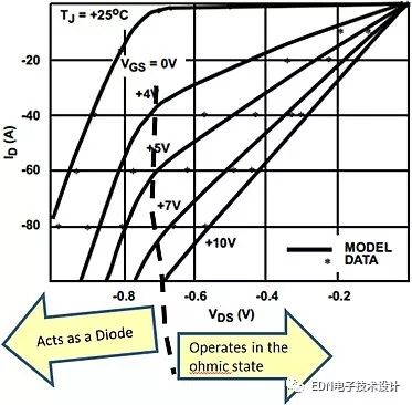
Figure 6: Typical characteristics of an N-channel MOSFET operating in the third quadrant when a gate voltage is applied.
Table 1 compares the N-channel MOSFET and the P-channel MOSFET.
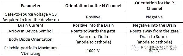
Table 1: Comparison of N-Channel and P-Channel MOSFETs.
cctv,cctv camera,outdoor,indoor,surveillance,home security
Dongguan Metalwork Technology Co., LTD. , https://www.dgdiecastpro.com