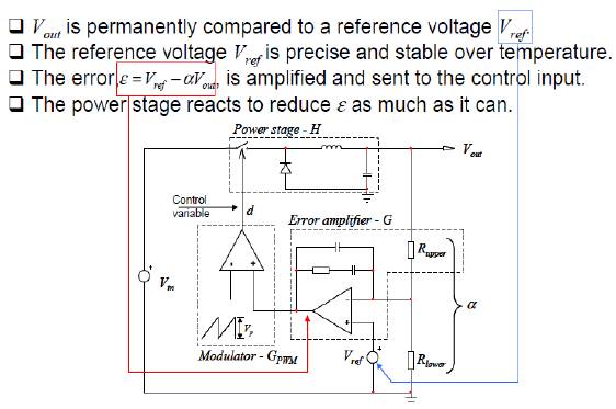
First, the relationship between loop and DC regulated power supply
Regulated power supply working principle
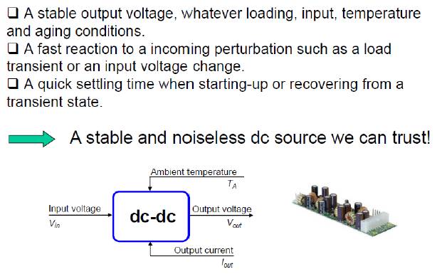
What kind of power supply do we need?
Second, the basic concepts related to the loop
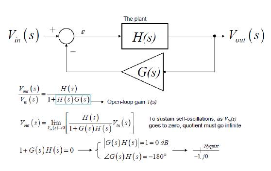
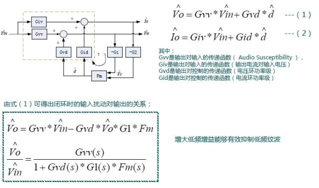
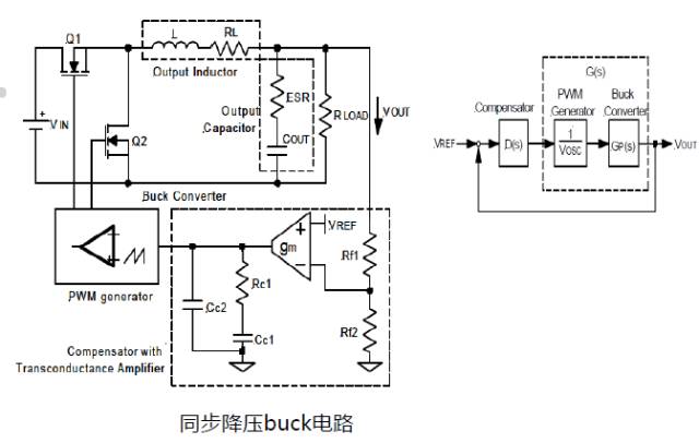
Power system block diagram
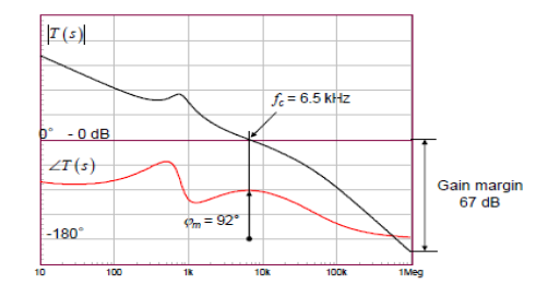
Bode diagram (determining steady-state margin from Nyquist diagram is very cumbersome)
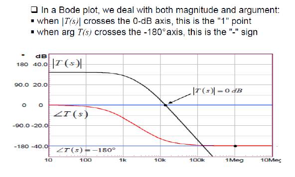
Crossover frequency and phase margin, gain margin
â– Crossover frequency: The frequency point at which the gain curve crosses the 0dB line
â– phase margin): the phase difference between the phase of the phase curve at the crossing frequency and -180 degrees
â– Gain margin: The gain of the gain curve at a frequency where the phase curve reaches -180 degrees.
Loop stability criterion
According to the Nyquist stability criterion, the system is stable when the phase margin of the system is greater than 0 degrees.
â– Guideline 1: At the crossover frequency, the total open loop system must have a phase margin greater than 30 degrees;
â– Criterion 2: In order to prevent the circuit phase of the -2 gain slope from changing rapidly, the open-loop gain curve of the system is near the crossing frequency.
The gain slope should be -1 (-20db/10 octave)
â– Criterion 3: Gain margin is a measure of the modulus of an open-loop system that may cause the curve to pass just -1 point. A gain margin of 6 db is generally required.
Remarks: It should be noted that it is not absolutely required that the gain slope of the open-loop gain curve near the crossing frequency must be -1, but since the phase curve corresponding to the -1 gain slope has a small phase delay and the change is relatively slow, it can guarantee When the phase change of some links is ignored, the phase curve will still have enough phase margin to keep the system stable.
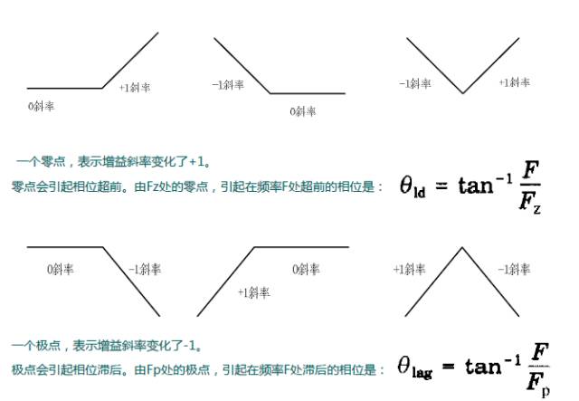
To meet the above three criteria, we need to know the gain and phase of all aspects of the open-loop system, introduce a transfer function, the concept of zero-pole can analyze this problem well. . .
Transfer function zero pole
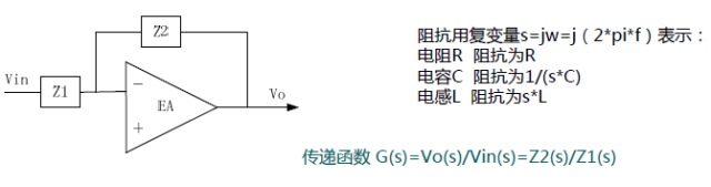
If the input and feedback branches are made up of different resistors and capacitors, the amplitude and phase frequency curves will take many forms.
The impedances Z1 and Z2 are represented by complex variables s(s=jw), and after a series of mathematical operations, the transfer function will be obtained. The gain/phase curve can be plotted by the transfer function.
Through algebraic operations, G(s) is expressed as G(s)=N(s)/D(s), and its numerator and denominator are functions of s.
Then the factor and the denominator are factorized and expressed as the product of multiple factors, ie
G(s)=N(s)/D(s)=[(1+s/2*pi*fz1)(1+s/2*pi*fz2)(1+/2*pi*fz3)]/
[(s/2*pi*f0)*(1+s/2*pi*fp1)*( 1+s/2*pi*fp2)* (1+s/2*pi*fp3)],
The corresponding frequency fz in the numerator is zero point frequency, and the corresponding frequency in the denominator is called fp as the pole frequency. F0 is called the initial pole.
Gain slope change rule caused by zero-pole frequency
Try to analyze a Type II compensator with a zero pole

The setting of the corner frequencies Fz and Fp.
The further the distance between Fz and Fp, the greater the phase margin. This will reduce the low frequency gain and reduce the attenuation of the low frequency ripple. As the high frequency gain increases, high frequency narrow noise spikes pass through at a greater amplitude. If Fz is at Fz2 and no longer Fz1, the gain at low frequency F1 is G1 instead of G2; if Fp is at Fp2 and no longer Fp1, the gain at high frequency Fh is G3 instead of G4.
Low frequency gain and ripple relationship
Small signal model
Third, the commonly used compensation controller
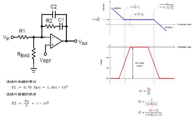
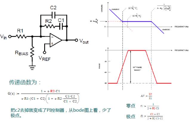
Commonly used compensation controller - Type II
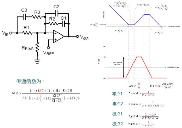
Commonly used compensation controller - Type III
Fourth, the analog loop design process
Analog loop design flow
1. Collect system parameters such as input voltage, output voltage, filter parameters, etc., and determine the switching frequency.
2. Determine the poles of the power stage
3. Determine the type of crossing frequency and compensator
4. Determine the zero pole of the required compensator
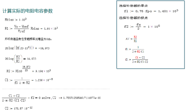
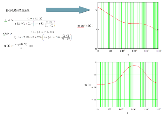
5, calculate the actual resistance and capacitance parameters
Design Example - A Simple Synchronous Buck Buck Circuit (Voltage Type)
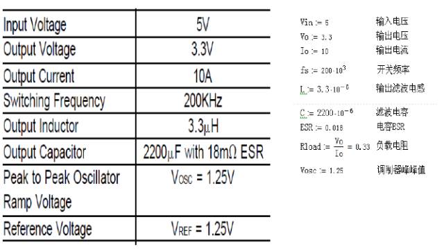
Step 1: Collect system parameters
Step 2: Determine the poles of the power stage
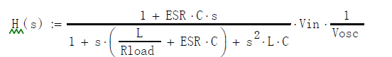
The double pole caused by the output filter inductor and capacitor:
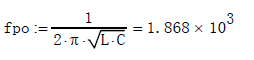
Zero point caused by output capacitor RSR
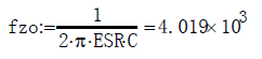
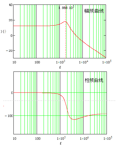
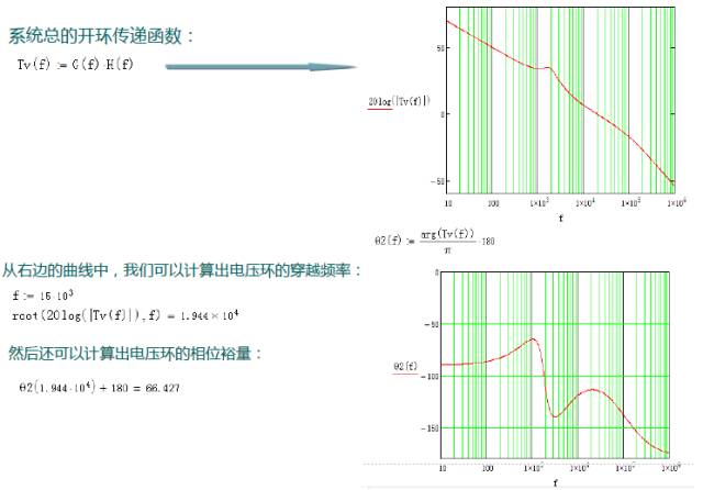
From the above curve, we can calculate the crossing frequency of the voltage loop:

Then you can also calculate the phase margin of the voltage loop:

Question: So far the open loop system has been stable, do you still need to design a loop?
Step 3: Determine the type of crossing frequency and compensator
According to the sampling theorem, the crossing frequency (fc) must be less than 1/2 of the switching frequency, but in reality the crossing frequency must be much less than 1/2 of the switching frequency, otherwise there will be a large switching ripple in the output. Here the switching frequency is 200k, we choose to cross the frequency 20KHz (1/10 switching frequency).
Because fpo Step 4: Determine the zero pole of the required compensator Step 5: Calculate the actual resistance and capacitance parameters Bode diagram of compensator System open loop bode diagram All In One Computer Core I5,I5 8Gb All In One,30 Inch All In One Computer,30 Inch All In One Desktop Guangdong Elieken Electronic Technology Co.,Ltd. , https://www.elieken.com